
2D semiconductors are only half the story ...
2D materials need new types of insulators if we are to produce ever smaller generations of efficient and powerful electronic components
For a long time, something important has been neglected in electronics, according to a team at the Faculty of Electrical Engineering at the TU Wien (Vienna). That is, if you want to keep shrinking semiconductor chips, you need the right insulator materials. Tibor Grasser and Yury Illarionov have recently analysed how to solve this problem in the journal Nature Communications.
The FET is the fundamental building block for information processing and storage. A FET works by controlling the current flow along a conductive surface channel formed between source and drain electrodes when a voltage is applied to the gate electrode, which is separated from the channel by an insulating layer (dielectric).
The performance of FETs strongly depends not only on the properties of the channel material (e.g. its carrier mobility), but also on the quality of the interface to the gate insulator and the overall properties of that insulator.
The last decade has seen a frantic search for channel materials with higher mobilities than silicon in ultrathin layers to keep up scaling according to Moore’s law. As an attempt to address this limitation, 2D semiconductors, such as MoS2, other transition metal dichalcogenides (TMDs, e.g. MoSe2, MoTe2, WS2, WSe2) or black phosphorus (BP), have been recently demonstrated as the great hope for channel materials in FETs.
At a first glance, 2D materials seem to allow the arbitrary stacking of different material layers using van der Waals attractive forces. And theoretical calculations have predicted excellent properties for devices built from 2D materials. Also, considerable progress has been made in addressing fabrication-related issues and tuning electrical figures of merit, such as carrier mobility and on/off current ratios.
However, published 2D devices often suffer from non-competitive carrier mobilities, subthreshold swings (SS) and drifts of important device parameters (e.g. the threshold voltage shift over time), which may have nothing to do with 2D semiconductors, but arise from the gate insulators used. As a result, there is still no commercially competitive 2D transistor technology available today.
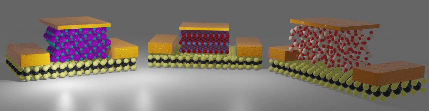
Currently, only a small selection of insulators for extremely small transistors exists. Pictured above are SiO2 (right) which is amorphous and has an undefined surface, hBN (middle) wiuch is crystalline but it is not a good insulator, CaF2 (left) is crystalline, has a clean surface, and is a very good insulator.
"The semiconductor industry today uses silicon and silicon oxide," says Tibor Grasser from the Institute of Microelectronics at the TU Wien. "These are materials with very good electronic properties. For a long time, ever thinner layers of these materials were used to miniaturise electronic components. This worked well for a long time - but at some point we reach a natural limit".
"2D materials are only the first half of the story," says Grasser. "The materials have to be placed on the appropriate substrate, and an insulator layer is also needed on top of it - and this insulator also has to be extremely thin and of extremely good quality, otherwise you have gained nothing from the 2D materials. It's like driving a Ferrari on muddy ground and wondering why you don't set a speed record."
"Silicon dioxide, which is normally used in industry as an insulator, is not suitable in this case," he continues. "It has a very disordered surface and many free, unsaturated bonds that interfere with the electronic properties in the 2D material."
It is better to look for a well-ordered structure: The team has already achieved excellent results with special crystals containing fluorine atoms. A transistor prototype with a calcium fluoride insulator has already provided convincing data, and other materials are still being analysed.
"New 2D materials are currently being discovered. That's nice, but with our results we want to show that this alone is not enough," says Grasser. "These new electrically conductive 2D materials must also be combined with new types of insulators. Only then can we really succeed in producing a new generation of efficient and powerful electronic components in miniature format".
'Insulators for 2D nanoelectronics: the gap to bridge' by Yury Yu. Illarionov et al; Nature Communications volume 11, Article number: 3385 (2020)


