
Korean team looks to perovskite for next gen memories
2D layered-structure perovskite device maintained memory characteristics over 140 degC and could be operated at voltages lower than 1V
A research team at the Pohang University of Science and Technology (POSTECH) in Korea has made a memory device using a 2D layered perovskite material, unlocking the possibility of commercialising a next-generation memory device that can be operated at low power.
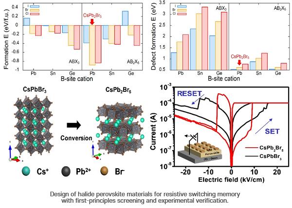
The team consisting of Jang-Sik Lee of the Department of Materials Science and Engineering, Donghwa Lee of the Division of Advanced Materials Science, Youngjun Park, and Seong Hun Kim in the PhD course succeeded in designing an optimal halide perovskite material (CsPb2Br5) that can be applied to a ReRAM device by applying the first-principles calculation based on quantum mechanics. The findings were published in Advanced Science.
The ideal next-generation memory device should process information at high speeds, store large amounts of information with non-volatile characteristics where the information does not disappear when power is off, and operate at low power for mobile devices.
The recent discovery of the resistive switching property in halide perovskite materials has led to worldwide active research to apply them to Resistive Random Access Memory (ReRAM) devices. These are non-volatile memories operated using the phenomenon where the resistance state changes from high to low, or from low to high depending on the applied voltage. However, the poor stability of halide perovskite materials when they are exposed to the atmosphere have been raised as an issue.
The research team compared the relative stability and properties of halide perovskites with various structures using the first principles calculation. DFT calculations predicted that CsPb2Br5, a 2D layered structure in the form of AB2X5, may have better stability than the 3D structure of ABX3 or other structures (A3B2X7, A2BX4), and that this structure could show improved performance in memory devices.
To verify this result, CsPb2Br5, an inorganic perovskite material with a 2D layered structure, was synthesised and applied to memory devices for the first time. The memory devices with a 3D structure of CsPbBr5 lost their memory characteristics at temperatures higher than 100degC. However, the memory devices using a 2D layered-structure of CsPb2Br5 maintained their memory characteristics over 140 degC and could be operated at voltages lower than 1V.
Jang-Sik Lee who led the research commented: "Using this materials-designing technique based on the first-principles screening and experimental verification, the development of memory devices can be accelerated by reducing the time spent on searching for new materials.
"By designing an optimal new material for memory devices through computer calculations and applying it to actually producing them, the material can be applied to memory devices of various electronic devices such as mobile devices that require low power consumption or servers that require reliable operation. This is expected to accelerate the commercialisation of next-generation data storage devices."
'Metal‐Halide Perovskite Design for Next‐Generation Memories: First‐Principles Screening and Experimental Verification' by Ju‐Hyun Jung et al; Advanced Science, https://doi.org/10.1002/advs.202001367


