
Osram presents infrared laser bars for metal processing
EKOLAS research project leads to novel laser bars with high values in efficiency and performance
Osram Opto Semiconductors has been working for many years on high-power lasers for special applications such as metal processing using welding robots in the automotive industry. Osram, along with its partners, is now presenting the results in laser bars’ performance and efficiency from the latest EKOLAS project funded by the German Federal Ministry of Education and Research.
In recent years, state-of-the-art laser technology has increasingly become an indispensable component of various industries – from medical technology to car manufacturing. The EffiLAS association is focused on securing and further expanding Germany's leading technological and economic position in photonics. In regard to the laser light sources the aim is to further optimise various parameters like performance and energy efficiency.
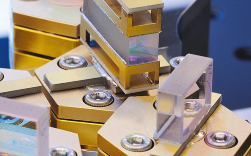
Together, with its partners Laserline, Heraeus, Fraunhofer ILT, fiberware and Welser Profile, Osram Opto Semiconductors has worked on various assignments in the EffiLAS joint project EKOLAS. The main aim was to develop highly efficient infrared laser bars with outstanding output powers and to demonstrate them in industrial materials processing. About 10 years ago, the best laser bars achieved a power of 200 watts with an efficiency of about 63 percent. Five years later, an output of 250 watts at an efficiency of no less than 60% was expected to be the limit of what could be achieved with the existing technologies. Conversion efficiency and cooling limited the output power of lasers at that time. The EKOLAS project, which was completed in February 2020, led to an infrared laser bar with an impressive maximum output of 400 watts in continuous wave operation. With an output of 300 watts, the bar sets a new standard with an efficiency of about 70 percent in the wavelengths of 1000 and 1020 nanometers.
The project partners were able to draw on experience gained in other ventures under the EffiLAS umbrella organization including an understanding of materials science and simulation in the field of epitaxy, as well as fundamental expertise in chip and facet technologies. "We are very excited to achieve, and in some cases even exceed, all of our targets in this project," explains Sebastian Hein, EKOLAS Project Manager at Osram Opto Semiconductors. "The key to success was the development of innovative software tools for simulating the electro-optical properties of the lasers, which take into account the thermal distribution, temperature-dependent material properties and mode-dependent wave propagation in the resonator. These tools considerably accelerated and simplified the necessary test runs, making a fundamental contribution to the results of the project.”
The newly gained knowledge from the simulation of certain processes can now be transferred to other product groups and wavelengths in the range between 800 and 1060 nm. In addition to the advantages in product development, the results also strengthen and consolidate the establishment of supply chains in Germany and the rest of Europe, thereby sustainably strengthening the industrial location.


