
EVG completes new clean room facility
Newly opened Cleanroom V building nearly doubles cleanroom capacity and strengthens capabilities of NILPhotonics and Heterogeneous Integration Competence Centres
EV Group (EVG), a supplier of wafer bonding and lithography equipment for semiconductor, MEMS and nanotechnology markets, has completed construction of its new Cleanroom V building at its corporate headquarters in Austria.
Built from top to bottom with the latest cleanroom design and construction technology, the new building nearly doubles the cleanroom capacity at EVG's headquarters, and will be used for product and process development, equipment demonstrations, prototyping and pilot-line production services. The Cleanroom V building, which is part of a €30 million investment announced last year, will officially open in August.
The new Cleanroom V building is directly connected to EVG's existing cleanroom and applications lab, and provides approximately 620 square metres of additional Class 10 cleanroom floor space. The new building also houses a modern training centre with multiple dedicated areas for training customers and field service engineers on EVG equipment platforms. As part of the expansion investment, the existing cleanroom and applications lab facility have also been upgraded, including the creation of redundant systems to ensure the highest availability and new safety features.
EV Group personnel are finalising the interior of the new facility, which includes dedicated co-development areas. It will officially open in August.
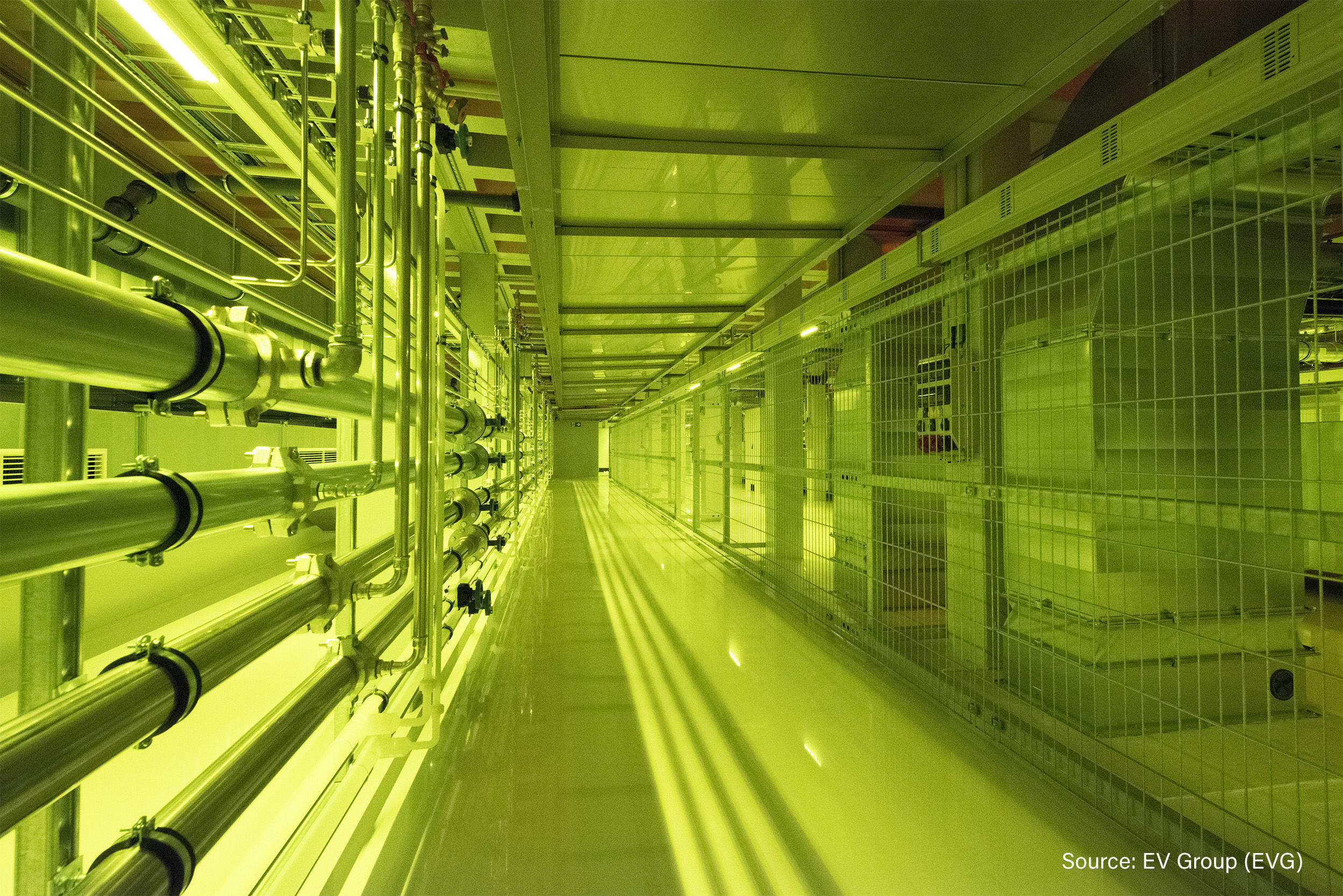
Pictured above is a behind-the-scenes look at the advanced sub-fab of EV Group's Cleanroom V facility, which has been designed with redundant systems to ensure the highest availability and new safety features.
Enhancing EVG's centres of technology excellence
The added capacity afforded by the new Cleanroom V building will strengthen the capabilities of EVG's NILPhotonics Competence Centre and Heterogeneous Integration Competence Centre, which provide world-class process development services, and serve as open access innovation incubators for customers and partners across the microelectronics supply chain.
Through these centres of technology excellence, EVG helps customers to accelerate technology development, minimise risk, and develop differentiating technologies and products through the implementation of nanoimprint lithography and heterogeneous integration, respectively, while guaranteeing the highest IP protection standards that are required for working on pre-release products.
"We are extremely proud of the technical innovation and know-how that went into the construction of this new cleanroom. It is truly a world-class, state-of-the-art facility down to the smallest details - arguably on par with some of the most technically advanced cleanrooms in Europe," stated Markus Wimplinger, corporate technology development & IP director at EV Group.
"For EVG, this new facility will greatly enhance our ability to co-develop future applications and technologies with our customers. In particular, we see it benefiting our Competence Centres, which have seen particularly strong activity and demand. The unique services offered at our NILPhotonics and Heterogeneous Integration Competence Centres enable our customers and partners to shorten development cycles and create novel products in these critical application areas."


