
Allos and KAUST collaborate on nitride red LEDs
Allos Semiconductors has engaged in a collaboration with Professor Ohkawa and his team at King Abdullah University of Science and Technology (KAUST) for realising high efficiency nitride-based red LEDs on large diameter silicon substrates.
In the collaboration the teams are addressing fundamental issues like the large lattice mismatch and the quantum-confined Stark effect (QCSE) which are preventing the adoption of red nitride-based LEDs for practical industry usage. In particular, for the emerging field of micro LED displays there is a strong demand to enable red LEDs on large diameter wafers in addition to the established blue and green color LEDs in the nitride system in order to reduce manufacturing complexity and cost.
In this context, Ohkawa and team have developed an InGaN-based red LED stack with low forward voltage of less than 2.5 V and high efficiency by using local strain compensation and a modified MOCVD reactor design. The researchers have already grown red LEDs on sapphire- and Ga2O3-substrates. For potentially higher performance red LEDs by using strain-engineering on wafer-level – in particular for large wafer diameters – the team is now extending its work to silicon substrates by collaborating with Allos.
This also enables huge advantages for mass production due to the scalability of up to 300 mm and thus processibility in silicon process lines. For micro LED displays – in particular the monolithically integrated micro displays for e.g. augmented reality (AR) application – this is another important enabler.

Figure 1: Allos’ in-line process control enables +/- 5 µm bow range
The unique high crystal quality of Allos’ GaN-on-Si technology with threading dislocation density (TDD) of ~2 x 108 cm-2 is the pre-condition to achieve at least the same performance red LED as on sapphire. Furthermore, Allos’ precise strain-engineering – which enables excellent emission uniformity for blue and green LED as well as flat bow wafer for 200 and 300 mm diameters – is used to optimise the growth conditions for red LED.
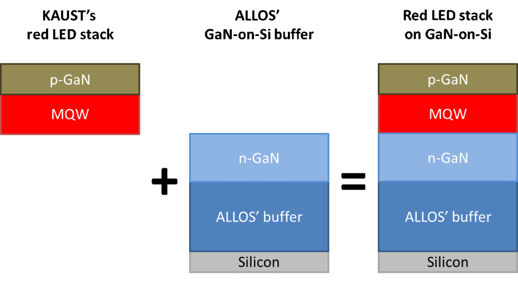
Both teams combine their echnologies to handle strain and optimise crystal growth conditions for GaN-on-Si and red LEDs. To this end, the KAUST team will grow its red LED stack on top of Allos’ GaN-on-Si-buffer layers, which will be fine-tuned during the collaboration to optimise the performance of KAUST’s red LED stack. The picture at the top shows how Allos’ established methods of integrating different LED stacks with its high crystal quality and strain-engineering buffer technology are used.
Dr. Nishikawa co-founder and CTO of Allos, commented: “From personal experience I am aware how challenging it is to realise high efficiency red LED. From Allos’ side we can provide our established blue and green high quality GaN-on-Si micro LED epiwafers of up to 300 mm diameter. Furthermore we see the opportunity that our unique strengths in strain-engineering can contribute to improved red LED performance.”
Commenting on the opportunity, Ohkawa said: “Our team has developed a high efficient red LED stack and continues to push the boundaries in this very challenging field. When talking to Allos, we of course were interested in the scalability up to 300 mm – but the capability to control the strain-engineering so precisely and in such a large process windows promises more progress for red LED performance.”
'633-nm InGaN-based red LEDs grown on thick GaN underlying layers with reducing in-plane residual stress' by D. Iida et al; Applied Physics Letters 116, 162101 (2020)
'Demonstration of low forward voltage InGaN-based red LEDs on β-Ga2O3 substrates', by D. Iida et al; Applied Physics Express 13, 031001 (2020)
'Metalorganic vapor-phase epitaxial growth simulation to realise high-quality and high-In-content InGaN alloys' by K. Ohkawa et al; Journal of Crystal Growth 512, pp.69-73 (2019)


