
Single-crystal perovskite devices closer to viability
Fabrication method results in flexible single-crystal films with controlled area, thickness, and composition
Nanoengineers at UC San Diego developed a new method to fabricate perovskites as single-crystal thin films, which are more efficient for use in solar cells and optical devices than the current state-of-the-art polycrystalline forms of the material.
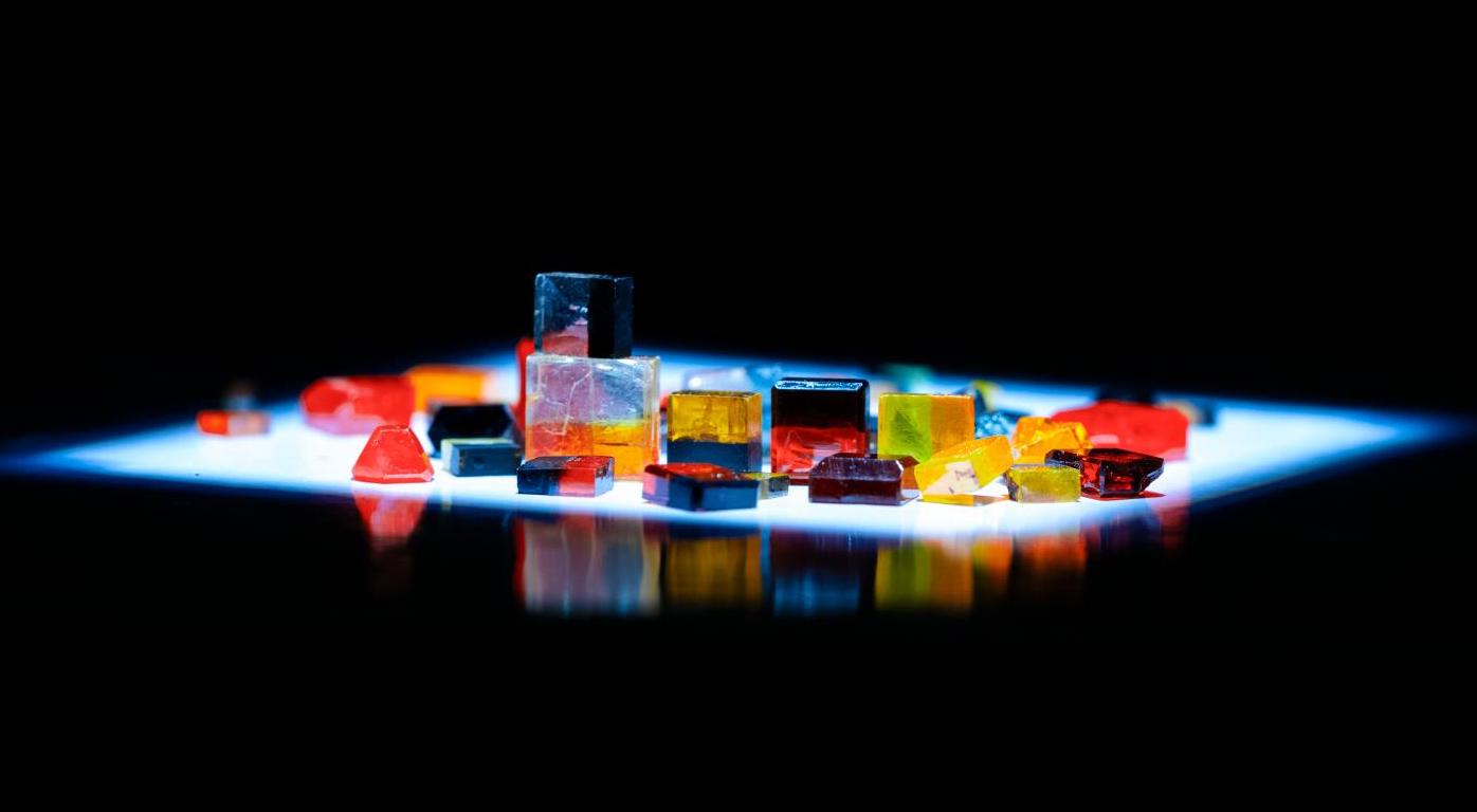
Their fabrication method - which uses standard semiconductor fabrication processes - results in flexible single-crystal perovskite films with controlled area, thickness, and composition. These single-crystal films showed fewer defects, greater efficiency, and enhanced stability than their polycrystalline counterparts, which could lead to the use of perovskites in solar cells, LEDs, and photodetectors.
Researchers in Sheng Xu's Jacobs School of Engineering nanoengineering lab published their findings on July 29 in Nature.
"Our goal was to overcome the challenges in realising single-crystal perovskite devices", said Yusheng Lei, a nanoengineering graduate student and first author of the paper. "Our method is the first that can precisely control the growth and fabrication of single-crystal devices with high efficiency. The method doesn't require fancy equipment or techniques--the whole process is based on traditional semiconductor fabrication, further indicating its compatibility with existing industrial procedures."
"Currently, almost all perovskite fabrication approaches are focused on polycrystalline structures since they're easier to produce, though their properties and stability are less outstanding than single-crystal structures", said Yimu Chen, a nanoengineering graduate student and co-first author of the paper.
Controlling the form and composition of single-crystal perovskites during fabrication has been difficult. The method invented in Xu's lab was able to overcome this roadblock by taking advantage of existing semiconductor fabrication processes including lithography.
"Modern electronics such as your cell phone, computers, and satellites are based on single-crystal thin films of materials such as silicon,GaN, and GaAs," said Xu. "Single crystals have less defects, and therefore better electronic transport performance, than polycrystals. These materials have to be in thin films for integration with other components of the device, and that integration process should be scalable, low cost, and ideally compatible with the existing industrial standards. That had been a challenge with perovskites."
In 2018, Xu's team was the first to successfully integrate perovskites into the industrial standard lithography process; a challenge, since lithography involves water, which perovskites are sensitive to. They got around this issue by adding a polymer protection layer to the perovskites followed by dry etching of the protection layer during fabrication. In this new research, the engineers developed a way to control the growth of the perovskites at the single crystal level by designing a lithography mask pattern that allows control in both lateral and vertical dimensions.
In their fabrication process, the researchers use lithography to etch a mask pattern on a substrate of hybrid perovskite bulk crystal. The design of the mask provides a visible process to control the growth of the ultra-thin crystal film formation. This single-crystal layer is then peeled off the bulk crystal substrate, and transferred to an arbitrary substrate while maintaining its form and adhesion to the substrate. A lead-tin mixture with gradually changing composition is applied to the growth solution, creating a continuously graded electronic bandgap of the single-crystal thin film.
The perovskite resides at the neutral mechanical plane sandwiched between two layers of materials, allowing the thin film to bend. This flexibility allows the single-crystal film to be incorporated into high-efficient flexible thin film solar cells, and into wearable devices, contributing toward the goal of battery-free wireless control.
Their method allows researchers to fabricate single-crystal thin films up to 5.5 cm by 5.5 cm squares, while having control over the thickness of the single-crystal perovskite--ranging from 600 nanometers to 100 microns--as well as the composition gradient in the thickness direction.
"Further simplifying the fabrication process and improving the transfer yield are urgent issues we're working on," said Xu. "Alternatively, if we can replace the pattern mask with functional carrier transport layers to avoid the transfer step, the whole fabrication yield can be largely improved."
Instead of working to find chemical agents to stabilize the use of polycrystalline perovskites, this study demonstrates that it's possible to make stable and efficient single-crystal devices using standard nanofabrication procedures and materials. Xu's team hopes to further scale this method to realise the commercial potential of perovskites.
'A fabrication process for flexible single-crystal perovskite devices' by Yusheng Lei et al; Nature, volume 583, pages790–795(2020)


