
How to build a better nanoscale LED
New design overcomes long-standing LED efficiency problem - and can transform into a laser
A new design for LEDs developed by a team including scientists at the US National Institute of Standards and Technology (NIST) may hold the key to overcoming a long-standing limitation in the light sources' efficiency. The concept, demonstrated with microscopic LEDs in the lab, achieves a dramatic increase in brightness as well as the ability to create laser light -- all characteristics that could make it valuable in a range of large-scale and miniaturized applications.
The team, which also includes scientists from the University of Maryland, Rensselaer Polytechnic Institute and the IBM Thomas J. Watson Research Center, detailed its work in a paper published today in the peer-reviewed journal Science Advances. Their device shows an increase in brightness of 100 to 1,000 times over conventional tiny, submicron-sized LED designs.
"It's a new architecture for making LEDs," said NIST's Babak Nikoobakht, who conceived the new design. "We use the same materials as in conventional LEDs. The difference in ours is their shape."
LEDs have existed for decades, but the development of bright LEDs won a Nobel prize and ushered in a new era of lighting. However, even modern LEDs have a limitation that frustrates their designers. Up to a point, feeding an LED more electricity makes it shine more brightly, but soon the brightness drops off, making the LED highly inefficient. Called "efficiency droop" by the industry, the issue stands in the way of LEDs being used in a number of promising applications, from communications technology to killing viruses.
While their novel LED design overcomes efficiency droop, the researchers did not initially set out to solve this problem. Their main goal was to create a microscopic LED for use in very small applications, such as the lab-on-a-chip technology that scientists at NIST and elsewhere are pursuing.
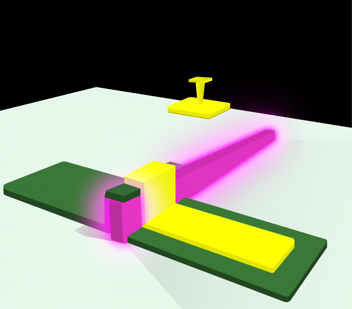
The team experimented with a whole new design for the part of the LED that shines: Unlike the flat, planar design used in conventional LEDs, the researchers built a light source out of long, thin zinc oxide strands they refer to as fins. (Long and thin are relative terms: Each fin is only about 5 micrometers in length, stretching about a tenth of the way across an average human hair's breadth.) Their fin array looks like a tiny comb that can extend to areas as large as 1 centimeter or more.
"We saw an opportunity in fins, as I thought their elongated shape and large side facets might be able to receive more electrical current," Nikoobakht said. "At first we just wanted to measure how much the new design could take. We started increasing the current and figured we'd drive it until it burned out, but it just kept getting brighter."
Their novel design shone brilliantly in wavelengths straddling the border between violet and ultraviolet, generating about 100 to 1,000 times as much power as typical tiny LEDs do. Nikoobakht characterises the result as a significant fundamental discovery.
"A typical LED of less than a square micrometer in area shines with about 22 nanowatts of power, but this one can produce up to 20 microwatts," he said. "It suggests the design can overcome efficiency droop in LEDs for making brighter light sources."
"It's one of the most efficient solutions I have seen," said Grigory Simin, a professor of electrical engineering at the University of South Carolina who was not involved in the project. "The community has been working for years to improve LED efficiency, and other approaches often have technical issues when applied to submicrometer wavelength LEDs. This approach does the job well."
The team made another surprising discovery as they increased the current. While the LED shone in a range of wavelengths at first, its comparatively broad emission eventually narrowed to two wavelengths of intense violet color. The explanation grew clear: Their tiny LED had become a tiny laser.
"Converting an LED into a laser takes a large effort. It usually requires coupling a LED to a resonance cavity that lets the light bounce around to make a laser," Nikoobakht said. "It appears that the fin design can do the whole job on its own, without needing to add another cavity."
A tiny laser would be critical for chip-scale applications not only for chemical sensing, but also in next-generation hand-held communications products, high-definition displays and disinfection.
"It's got a lot of potential for being an important building block," Nikoobakht said. "While this isn't the smallest laser people have made, it's a very bright one. The absence of efficiency droop could make it useful."
'High-brightness lasing at submicrometer enabled by droop-free fin light-emitting diodes (LEDs)' by B. Nikoobakht et al; Science Advances. August 14, 2020.


