
IGaN epi centre aims to boost GaN ecosystem in Asia
IGaN, IGSS Ventures and partners invest some $73 million to expand GaN epi production capacity
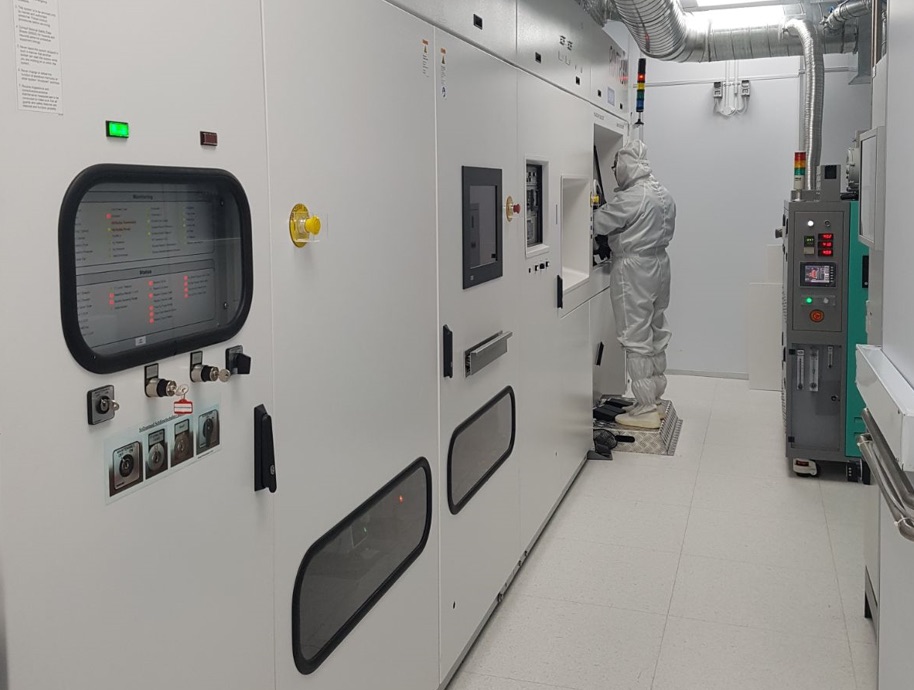
Following successes in customer pilot lines, Singapore-based IGSS GaN, a company focused on GaN-on-Si/SiC technology, has set up a 4inch to 8inch MOCVD GaN Epi Centre which is expected to be operational mid-2021.
The Epi Centre brings together customers, universities, research institutes and tool vendors to collaborate in the future development of GaN technologies as the quality of epiwafers are critical to GaN device manufacturing, according to Raj Kumar, IGaN’s CEO and founder of its holding company IGSS Ventures.
IGaN, IGSS Ventures and select partners have invested some $73 million to expand GaN epi production capacity and to mass produce 8inch GaN fabrication technologies.
“What the industry lacks today is a concerted effort to enhance the overall GaN ecosystem to lower cost barriers so that technology adoption can happen at the pace the market is moving. We projected more than nine years ago that at 8inch wafer dimensions, GaN-on-Si capabilities becomes a competitive and powerful solution to create the right balance between superior performances and cost competitiveness," said Kumar.
"A commercial centre and Joint Lab hosting several top specialist brands and leading vendors is a timely market response to creating strategic partnerships that fast-track innovation, growth, and customer value. Capitalising on the recognisable Singapore-brand, second to none IPs standards, its known semiconductor infrastructure and IGaN’s in-house expertise, I truly believe we can set standards, create benchmarks and lead the global movement in GaN adoption,” he added.
Ambitions for the Epi Centre is indicative of the growing excitement in the industry as GaN technology sits at the intersection of power-efficient electronics, AI, 5G and IoT, charging systems/powertrain management, green energy and smart city demands.


