
ACM Research introduces Cleaning System for ultra-thin Wafers
Patented touch-free Bernoulli handling and processing system supports wet processes for ultra-thin power wafers with high warpage
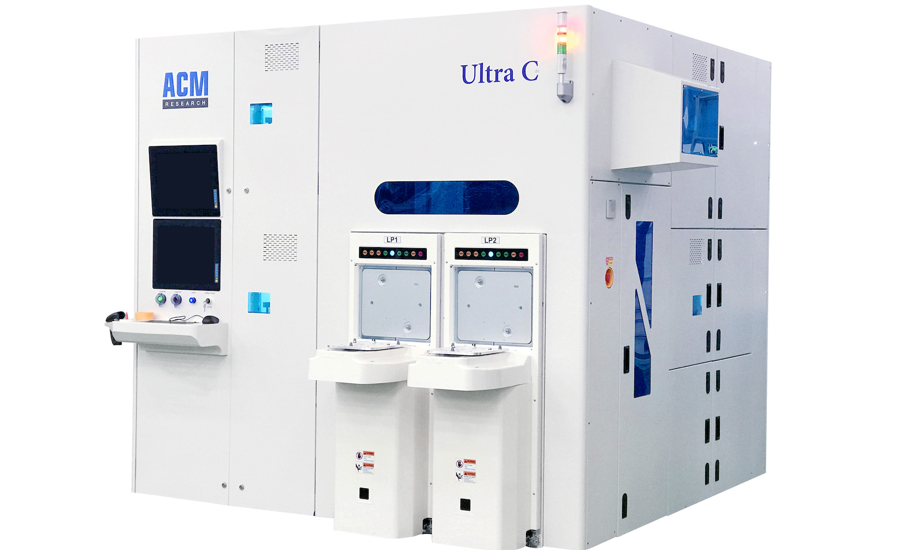
ACM Research, a supplier of wafer-processing systems, has introduced a Thin Wafer Cleaning System, a high-throughput, four-chamber system designed for single-wafer wet processes, including cleaning, etching and surface finishing.
The system is intended for the manufacture of both MOSFET and IGBT devices for the power semiconductor market, and features touch-free handling and processing based on the Bernoulli effect to eliminate possible wafer damage and improve final device yield. It supports 200mm and 300mm Si wafers and is suitable for Taiko wafers down to 50-micron thickness, ultra-thin wafers of less than 200-micron thickness, high aspect ratio (>10:1) deep-trench wafers as well as double-thickness bonded wafer pairs.
There is growing demand for smaller pitch, deeper trench and thinner wafers. Yole Développement, a market research and technology analysis firm, predicted that the market for thinned wafers will increase from 100 million in 2019 to 135 million in 2025, a compound annual growth rate (CAGR) of more than 5 percent. Yole Développement expects this market growth to be driven by memory, CMOS image sensors and power SiC components as well as LED and laser diodes.
“To compete for market share, power device manufacturers must expand their MOSFET and IGBT manufacturing lines to include wafer thinning equipment, without significantly increasing the overall fab footprint,” said David Wang, ACM’s CEO and President. “We have responded by developing a four-chamber tool that offers much higher throughput than the currently available two-chamber systems. Additionally, we outfitted the tool with a proprietary contactless handling and processing system to prevent these fragile wafers—which can be as thin as 50 microns—from being damaged during the backside thinning and cleaning processes, thereby increasing overall device yield.”
This new tool’s handling system is programmable to accommodate deep-trench, Taiko and ultra-thin wafers, or bonded wafers. The robot arms for loading and unloading, as well as the chuck, have been designed for non-contact wafer handling using a proprietary method based on the Bernoulli effect. Nitrogen gas (N2) provides constant pressure to keep the wafer floating in place on the arm, which can be flipped for processing on either side while still holding the wafer in place. This allows for handling high-warpage wafers without contact.
During the wet process, the wafer sits front-side down on a Bernoulli chuck, where an N2 flow cushions the wafer, protecting it and keeping it dry. This proprietary design, using ACM’s patented technology on a Bernoulli chuck, features a recipe-controlled gap between the wafer and chuck to meet requirements for undercut width control on the wafer device side edge, as well as pin-mark-free control. Additionally, the system can be configured to include an optional thickness measurement function.
ACM’s Thin Wafer Cleaning System has been designed to meet manufacturers’ needs. After mechanical grinding/polishing is performed to achieve desired thickness, ACM’s handling system supports these ultra-thin, high-warpage wafers throughout subsequent critical processes, including silicon thinning using a wet-etch step to eliminate microcracks. Additionally, by implementing a different combination of chemistries, this tool can be used for cleaning, photoresist removal, thin-film removal and metal etching.
Each chamber can be configured with up to four swing arms for delivering process chemistries such as wet etchants, solvents, RCA cleaning chemicals, deionized water and nitrogen. Additionally, the chambers are designed to allow reclaiming of two types of chemicals.
ACM delivered its first Thin Wafer Cleaning System to a China-based analogue/power semiconductor manufacturer in the second quarter of 2020.


