
NXP opens GaN Fab in Arizona
High-volume facility is thought to be the most advanced GaN fab for RF in the United States
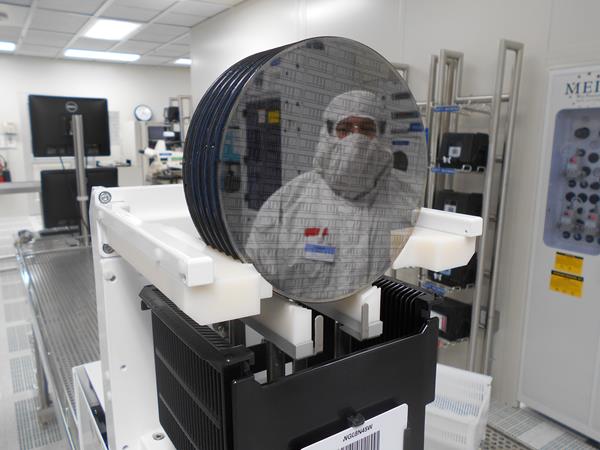
NXP Semiconductors has opened an 150 mm (6-inch) RF GaN fab in Chandler, Arizona. The new factory, which will support the expansion of 5G base stations and advanced communications infrastructure, is thought to be the most advanced GaN fab for RF in the US.
The opening ceremony was marked by keynote addresses and remarks by NXP executives plus federal, state and local government officials.
In his keynote address, Kurt Sievers, NXP CEO said: “Today marks a critical milestone for NXP. By building this incredible facility and tapping key talent in Arizona, we are able to bring focus to GaN technology as part of driving the next generation of 5G base station infrastructure.”
NXP has nearly 20 years of GaN development expertise and extensive wireless communication industry knowledge. The company has optimised its GaN technology to improve the electron trapping in the semiconductor to deliver high efficiency and gain with high linearity.
Joakim Sorelius, head of development Unit Networks at Ericsson, a longstanding NXP customer, commented: “We strive to deliver industry leading products that provide maximum value to our customers, where power amplifiers play an important part of the radio technology. Similar to Ericsson’s recent US investments, we are pleased to see NXP's investments in the US semiconductor process development with the continuous focus on improving RF system performance for future high demanding radio networks."
“I am excited by the opening of our new facility in Chandler as it underscores NXP’s decades-long commitment to GaN and the communications infrastructure market,” said Paul Hart, executive VP and GM of the Radio Power Group at NXP. “I would like to thank our customers for their collaboration throughout the years and the entire NXP team that has been instrumental in creating the world’s most advanced RF GaN fab, which is designed and ready to scale to 6G and beyond.”
The fab is set to ramp quickly with NXP using its Chandler-based team and their long-standing expertise in compound semiconductor manufacturing. Arizona Governor Doug Ducey added: “With this new state-of-the-art manufacturing facility in Chandler, Arizona is set to expand its reputation as a high-tech manufacturing hub and a pioneer in 5G innovation. We’re grateful to NXP for bringing more jobs and investment to our state.”
The internal factory will serve as an innovation hub that facilitates collaboration between the fab and NXP’s onsite R&D team. NXP engineers can now more rapidly develop, validate and protect inventions for current and future generations of GaN devices, resulting in shorter cycle times for NXP GaN innovations.
NXP’s new Chandler-based GaN fab is qualified now, with initial products ramping in the market and expected to reach full capacity by the end of 2020.


