
2D perovskite derivative shows potential for Valleytronics
Rice University team shows that layered compound of caesium, bismuth and iodine is adept at storing valley states of electrons in the structure's odd layers
Engineers at Rice University and Texas A&M University have found a 2D derivative of perovskite that they think could make computers faster and more energy-efficient. Their material has the surprising ability to enable the valleytronics phenomenon touted as a possible platform for information processing and storage.
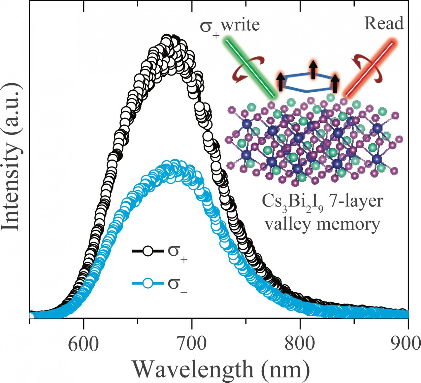
The lab of materials scientist Jun Lou of Rice's Brown School of Engineering synthesised a layered compound of caesium, bismuth and iodine that is adept at storing the valley states of electrons, but only in the structure's odd layers.
These bits can be set with polarised light, and the even layers appear to protect the odd ones from the kind of field interference that bedevils other perovskites, according to the researchers. Best of all, the material appears to be scalable.
"This is not a new material, but we figured out a way to make it without solution processing or exfoliating it from bulk," Lou said. "What's novel is that we can produce it (via chemical vapor deposition) in a few layers, and all the way down to a monolayer. That enabled us to probe its nonlinear optical properties."
The discovery is detailed in Advanced Materials.
Valleytronics are a cousin to spintronics, in which memory bits are defined by an electron's quantum spin state. In valleytronics, electrons have degrees of freedom in the multiple momentum states - or valleys - they occupy. These states can be read as bits.
"In a transistor, if you put an electron there, it represents a state, and if you take it out, that represents another state," said co-principal investigator Hanyu Zhu of Rice. "In valleytronics, the electrons are always present, and are in either of two different quantum wavefunctions with opposite momenta. These two wavefunctions interact with different light polarisation, so the momentum state can be resolved optically."
A close look at the inorganic, lead-free material through an electron microscope showed molecules in the odd layer are asymmetric. "That lack of symmetry is missing in the even layers - that's how we differentiate between them - and it gives rise to the properties we see," Lou said. "That's just the nature of this crystal structure."
The lab tested the material with up to 11 layers and found a lack of transparency doesn't seem to affect how well light triggered a response. "Even a thicker material behaves like it's still a single layer," Lou said. "That's quite important."
"Thicker 2D transition metal dichalcogenides lose unique properties like valleytronics," he said. "All the behaviors are gone. That's not the case for this material."
Lou said calculations by co-principal investigator Xiaofeng Qian of Texas A&M University provided the necessary theoretical evidence.
"The valley polarisation observed in both thin and thick layers is largely due to the weak interlayer electronic coupling, a unique feature of this perovskite derivative compared to other 2D materials when stacked together," Qian said. "It also leads to persistent nonlinear optical responses in thicker samples."
The material also seems less susceptible to environmental degradation, a common problem for hybrid perovskites developed for solar energy. "This material won't give you very high conversion efficiency, but think of it like an all-around athlete in the Olympic Games," said lead author and Rice postdoctoral fellow Jia Liang. "It may not be the best in each category, but if you consider its different aspects together, it will stand out," he said.
The researchers suggested the already strong light-matter interaction they observed could be enhanced by further engineering the material's band gap.
"I think it's a breakthrough for using this type of material in information processing," Lou said. "We're really hoping this is the starting point."


