
The evolution of the deep-UV LED
During the last 20 years deep-UV LEDs have been invented, improved, and commercialised, allowing them to replace mercury lamps in disinfection, polymer curing and skin treatment products
BY Asif Khan FROM THE University of South Carolina
The 1990s will be remembered for the birth of efficient blue and green LEDs based on GaN. In the decade that followed, further improvements came that you literally can’t see. This triumph resulted from extending the emission wavelength of GaN LEDs into the ultraviolet. Replacing the InxGa1-xN quantum wells with those made from AlxGa1-xN allowed devices to reach the ultraviolet realm, emitting in regions known as the UVB (315 nm to 280 nm) and the UVC (280 nm to 100 nm).
Further progress has followed, and today several companies from around the world are pursuing large-scale manufacturing and commercialisation of these solid-state sources, which are being deployed in many applications. Here, we provide an overview of this progress, including details of the accomplishments of several groups making major contributions. We begin with a historical perspective, before providing an account of the current-status, the emerging applications, and finally some of the latest research directions.
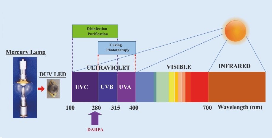
Figure 1: Solar spectrum and important application areas for UV LEDs. Shown is the wavelength requirements for the various application systems.
The primary motivation for making LEDs that emit below 365 nm is the creation of a superior alternative to the mercury lamp. This incumbent source for air-water purification, food disinfection and other bio-medical applications is bulky, fragile, requires a high operating voltage and comes with environmental concerns, as mercury can wreak havoc in food, water, and bio-medical industries. Producing high-efficiency, high-power LEDs operating in the UVB and UVC offers the potential to net substantial revenue, because such sources could address a variety of critical applications (see Figure 1). Helping to drive their incorporation is their compactness, long lifetime, the option for pulsed operation, and the ease with which they can be integrated with silicon electronics.Major milestones
Two trailblazers of the UV LED are our team from the University of South Carolina, and the group at NTT, Japan. At the beginning of 2001 NTT reported a device emitting at 346 nm, and shortly after we unveiled an LED with a peak output at 341 nm. These two devices broke new ground, featuring the first active regions made from the pairing of AlGaN and AlInGaN layers. Before the year was out, we had made further progress, realising 315 nm emission, the edge of the UVB domain. And a year later, we eclipsed that success, reporting an LED with a milliwatt output power, emitting at 278 nm, just inside the UVC band.
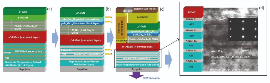
Figure 2: (a) Device epilayer structures for the first-generation devices. (b) Epilayer design for second-generation devices that produce 1 mW, and have an external quantum efficiency (EQE) of 1 percent. The arrows (1 through 4) depict the key design changes that led to the higher power and EQE values. (c) Device configuration with flip-chip geometry. (d) Transmission electron microscopy of the nested short period superlattices used in the formation of strain/defect mitigation AlN/AlGaN superlattices.
All these LEDs had the same architecture. At their heart lay an AlGaN multi-quantum well surrounded by n- and p-type AlGaN layers. Capping the p-side were p+-GaN layers, bolstering hole injection. These LEDs were built on sapphire substrates, coated with AlN buffer layers just 0.1-0.2 μm-thick, formed by moderate-temperature pulsed epitaxy. To improve material quality, they featured AlGaN/AlGaN superlattices. Combining dislocation filtering with strain management, these superlattices provided a foundation for the growth of n+-AlGaN (n-contact) layers with thicknesses exceeding 2 μm.Like many first-generation LEDs, these devices had a very low external quantum efficiency. Four factors were to blame: extended defects, resulting from lattice-mismatched growth of AlN/AlGaN layers on sapphire; a low doping efficiency, prevalent in p-AlGaN layers; the absorption of many of the photons exiting the quantum wells by hole-supplying p+-GaN; and a low light-extraction efficiency, exacerbated at the very shortest wavelengths.
By tackling these issues, the developers of UV LEDs made much progress over the next two years. For our team, as well as several other US institutions, efforts were supported by DARPA and the US Army. These bodies funded the SUVOS programme, managed by Lt. Col John Carrano. During SUVOS, we improved our materials, their growth, and the design and packaging of our device. These modifications created devices with an external quantum efficiency around 1 percent and an output power of nearly 1 mW at a 25 mA drive current.
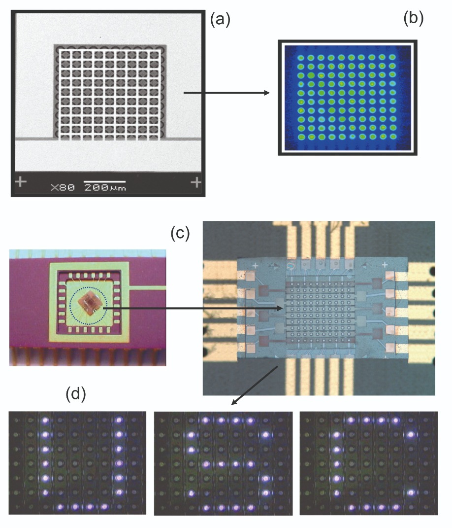
Figure 3: A 10 x 10 array micropixel LED that emits at 280 nm. (a) a scanning electron microscopy image of a 280 nm deep-UV LED with a 10 x 10 micropixel array. Each pixel diameter is approximately 30 μm. (b) the image of the micropixel LED under bias showing a uniform emission. (c) a fully packaged device mounted on a dual in-line package, along with a zoomed-in device image, clearly showing the electrode geometry for the matrix addressing of the deep-UV LED pixels. (d) with a controlled biasing, the 7 x 9 pattern micropixel LED can be used for a UVC display, in UVC communication systems and for deep-UV photolithography systems.
Better performance resulted from a combination of: high-temperature, migration-enhanced pulsed epitaxy for the growth of AlN buffer layers, which have a thickness in excess of 2 μm; the introduction of a nested superlattice for the AlGaN layers of the AlN/AlGaN superlattices; inclusion of a magnesium-doped, electron-blocking AlGaN layer; incorporation of polarization-doped, graded-composition p-AlGaN layers (see Figures 2 (a) and 2 (b)); and flip-chip mounting of the devices on metallic carriers (see Figure 2 (c)).
As just mentioned, one of the features of our second-generation devices is an improved superlattice design that aids defect and strain management and boosts output power (Figure 2 (d)). In this refined architecture, the AlN/AlxGa1-xN superlattices are nested short-period superlattices. They are formed using an aluminium-composition of the AlxGa1-xN layer of the macro-superlattice that is a thickness-averaged composition of the nested short-period AlxGa1-xN/AlyGa1-yN superlattices. By adopting this approach, we could grow crack-free, high-quality n+-AlxGa1-xN (n-contact layers) with thicknesses well over 2 μm. Incorporating this layer into our LEDs increased current spreading, mitigated current crowding and increased the current at which power-saturation kicked in. Thermal management also improved, leading to a longer device lifetime.
Substantial progress followed. By 2005, we were able to report the stability of our devices and their suitability for bio-chemical detection. Our demonstration of high-power, stable UVC LEDs provided a tremendous foundation for their commercialisation in applications that included air and water purification. While these devices are now well off the pace, the level of performance they provided is very effective in killing viruses and bacteria such as Ecoli.
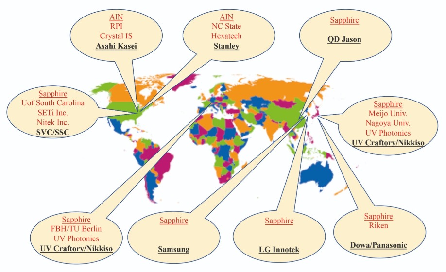
Figure 4: Global Partnerships for deep-UV LED development. Also shown is the substrate material that each team uses.
In addition to making significant contributions to the development of conventional, large-area UVC LEDs, we have also demonstrated a micropixel device. This configuration, reported in 2004, aids thermal management. Devices run cooler due to a reduction in total device resistance, a measure that combats current crowding and joule heating. Another merit of the micropixel device is that it allows biasing of individual pixels, making it ideal for deep-UV LED displays, UVC optical communication and deep UV lithography systems (see Figure 3). For the growth of UV LEDs, the most common substrate is sapphire. This material is transparent, low in cost, widely availability, and when used in combination with AlN buffer layers, it provides a good foundation for UV emitters. However, two US groups that manufacture bulk AlN substrates – Crystal IS and Hexatech Inc – have explored the potential of this platform for deep-UV LEDs. Note that other groups have not participated in this evaluation, due to the high cost and limited availability of AlN substrates. Although the use of native AlN has promise, one issue with bulk material is that during its growth, impurities are incorporated that have strong absorption in the UVC band.
Commercial conquests
Within the deep-UV LED community, university research groups have driven development. Their knowledge has transferred to start-ups, driving early commercialisation. More recently, several start-ups have formed partnerships, or been acquired by large companies.
Our team started this trend. Our deep-UV LED technology has been behind the launch of SETi and Nitek Inc, two small businesses in Columbia, South Carolina, that have been bought by Seoul Viosys Company and Seoul Semiconductors, respectively. In a similar vein, the technology from Nagoya University and Meijo University spawned UV Craftory Company, a start-up subsequently acquired by Nikkiso/FPG. Meanwhile, Riken’s technology has been directly acquired by DOWA/Panasonic; and more recently, in Germany, the technology from TU Berlin/FBH has been transferred to UV Photonics.
It’s a similar state of affairs for deep-UV LEDs developed on substrates made of AlN. Technology invented at Rensselaer Polytechnic Institute underpinned the launch of Crystal IS, which has been acquired by Asahi Kasei. Likewise, research at NC-State created Hexatech, now part of Stanley. In addition, large corporations, such as Samsung, LG Innotek, QD Jason and Nichia Corporation, have also started to venture into the deep UV.

Figure 5: Different packaging schemes employed for deep-UV LEDs. Shown are (a) various TO-headers; (b) custom aluminized headers for better light extraction; (c) LED chip on board (International Light Corporation (web-site)); and (d) packages with epoxy and quartz domes.
Today, nearly all the reported deep-UV LEDs share much of the structure found in those early devices, depicted in Figure 2 (b). But they often have one key difference. In many cases, out go the thin AlN buffer layers and AlGaN short-period superlattices that offer strain management, and in their place comes a thick, fully relaxed AlN buffer layer, followed by AlGaN superlattices and thick n+-AlGaN n-contact layers. The latter can be relaxed or pseudomorphic.Many different approaches are adopted for forming relaxed, thick AlN buffers. Such buffers are highly desirable, because their lower threading dislocation density lowers the defects in the active region and increases the LED’s internal quantum efficiency.
We are growing these buffers by high-temperature pulsed epitaxy and hydride vapor phase epitaxy, while researchers at Riken are creating them by ammonia flow modulation epitaxy and a team at TU Berlin is producing them by migration-enhanced lateral epitaxial overgrowth and the use of ex situ high-temperature-annealed sputtered AlN.
Commercial progress with deep UV LEDs has led to the launch of devices emitting between 240 nm and 300 nm. Despite significant progress, the external quantum efficiency of these devices and their wall-plug efficiencies fall well short of the figures for their visible counterparts. While InGaN-based blue LEDs realise figures of around 80 percent for these measures of efficiency, values for deep UV LEDs emitting between 266 nm and 300 nm are typically just 5-6 percent.
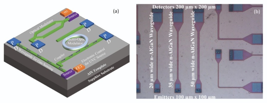
Figure 6: (a) schematic of a photonic integrated circuit (PIC) using the thick AlN on sapphire templates that are used for deep-UV LED epilayers. (b) A UVC PIC consisting of a UVC LED and UVC p-n junction detector connected using ridge waveguides.
Although efficiencies are inferior, like their visible cousins, lifetimes of deep UV LEDs are impressive. They are typically 10,000 hours, enabling use in air-water purification, sterilisation, polymer curing and phototherapy (see box “Uses of UV LEDs” for details).As the emission wavelength shortens, the external quantum efficiency of deep-UV LEDs falls, along with its wall-plug efficiency. This is partly due to degradation of material quality, and difficulties in doping nitride-based alloys with increased aluminium composition. In addition, according to a team at Kansas State University, once emission drops below 270-280 nm, transverse magnetic-polarized emission becomes more dominant, due to a reordering of the valence bands. As this form of light travels lateral to the c-plane, it is efficiently trapped in the device, hampering photon extraction.
Today, there is a wide variation in the packages and form factors of commercial deep-UV LEDs. Discrete devices are available in TO-39 packages. This is not suitable for large devices, which require superior thermal management. These chips are housed in SMD packaging with AlN sub-mounts. Recently, there has also been the introduction of devices incorporating UV-transparent epoxy encapsulation (see Figure 5 for images of the different device packaging schemes).
For everyone working in the field of deep UV LEDs, the biggest challenge is to increase device performance to values comparable with visible counterparts. Today’s device design for commercial products has two major drawbacks. First, the p+-GaN hole injection layer leads to a loss of light travelling towards the p-contact and the wave-guided light in the active region. Second, light extraction efficiency is very low.
Approaches to mitigate light absorption by the p+-GaN layer and extract/collect more light travelling towards the p-electrode include the use of p-AlGaN layers. This approach has been pioneered by a partnership between Sensor Electronic Technology, Rensselear Polytechnic Institute and the US Army Research Laboratory; and also a Japanese collaboration led by RIKEN that has employed reflective p-contacts. Both teams have realised external quantum efficiencies as high as 10 percent.
Even greater success has come from RIKEN, working with Eco Solutions Company, part of Panasonic Corporation. They have reported external quantum efficiencies of 20 percent, realised by combining patterned-sapphire substrates and transparent p-AlGaN contact layers.
Future directions
It not surprising that by and large, the development of AlGaN-based deep UV LEDs is mirroring that of InGaN-based visible LEDs. The latter now incorporates tunnel junctions, a technology starting to be explored in deep-UV LEDs. By adding MBE-grown, UV-transparent AlGaN tunnel junctions contacts made from n++/p++-Al0.15Ga0.85N to MOCVD-grown active layers, researchers at The Ohio State University have doubled the output power and the external quantum efficiency of LEDs emitting in the 280-290 nm range.
Another area of research is deep ultraviolet integrated optics. Here, efforts involve integrating UVC optical and electronic components on a chip using UVC transparent waveguides made from AlN or aluminium-rich AlGaN. Our team, and a collaboration led by researchers at Nanjing University of Posts and Telecommunications, have provided initial demonstrations of the integration of UVC LEDs and detectors with planar and channel waveguides (see Figure 6 (a), detailing the device integration approach, and Figure 6 (b), an image of an integrated UVC LED/detector).
Successes like this have contributed to the tremendous development in deep-UV LEDs over the last 20 years. This device is already serving some applications, and as its robustness increases, along with its output power and its cost-competitiveness, its deployment will surge. The path that the deep-UV LED will take will essentially follow that of its blue predeccesor. It is traveling faster at some stages, taking just five years from the initial demonstration in 2002 to the first commercial products. However, another ten years elapsed for technology scale-up and power and efficiency improvements, all essential ingredients for the manufacture of low-cost devices delivering sufficient performance. Once new insights in the development of these devices are integrated into large-scale production, this should lead to a hike in the efficiency of commercially available deep-UV LEDs. We have come a long way in the last 20 years, and in the new two decades we should go far further.
APPLICATIONS of deep-UV LEDs can be grouped into disinfection, bio-medical instrumentation, polymer curing and bio-chemical sensing.
Due to the blocking of solar radiation in the UVC band by the earth’s ozone layer, most living organisms don’t have survival mechanisms to cope with the exposure of radiation in this spectral range. When organisms are exposed, changes to RNA/DNA take place, and impair reproduction.
Due to this, organisms become inactive. Note that different organisms require different dose levels, and to some extent, carefully selected wavelengths. When organisms are exposed to UVC LEDs producing an output of 100-125 mW and a peak wavelength of about 265 nm, a flux of 40-50 mJ.cm-2 results that can incapacitate most bacteria, spores, and viruses. Several UVC LED companies, or their strategic partners, now sell systems based on UVC LEDs for purification. They can be used for point-of-use water purification of moderate volumes of water.
More recently, companies have started to investigate the use of UVC radiation for surface decontamination of viruses, such as Covid-19. Taking the lead is the Seoul Viosys Company. Its Violeds deep-UV LED technology is being incorporated in the Fresh Air brand of air-conditioners, manufactured by ‘Gree Electric Appliance Inc’, the largest Chinese manufacturer of air conditioners. Another adopter of this type of technology is the RGF Environmental Group, a leading in-duct air treatment supplier in the US. Such efforts demonstrate that deep-UV LED technology provides protection against a variety of harmful organisms.
Another class of deep-UV LED applications is polymer curing. When UVA/B/C radiation reaches polymers, this initiates chemical reactions. What happens is that the exposure of photo-initiator molecules creates free radicals, which drive the polymerization of monomer and oligomer molecules. Curing applications are the backbone of key industries such as coatings, ink printing, adhesives, and photolithography.
Deep UV LEDs are also very effective at generating photochemical reactions in living organisms. LEDs that emit in the UVB are an excellent source for enhancing the concentration of metabolites. This means that plant growth cycles, flavour and quality can be controlled using deep-UV light exposure. As well as bringing an economic benefit, this allows these sources of UV light to have far reaching implications for fighting global food shortages.
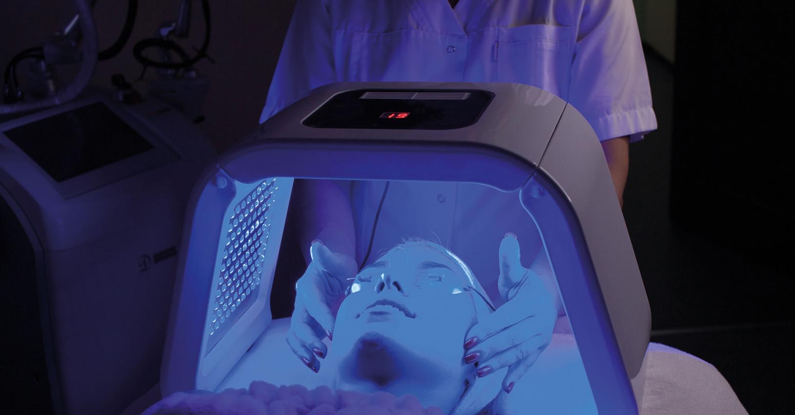
Phototherapy systems provide yet another commercial opportunity for deep-UV LEDs. These systems are currently in use to treat vitamin D deficiency, seasonal effective disorder, and psoriasis.
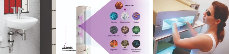
A point-of-use water purification system (left). A list of viruses and bacteria that the air-conditioning systems with incorporated UVC LED array can mitigate (middle). A UVB LED based psoriasis treatment system (right).
Submilliwatt operation of AlGaN-based ultraviolet light-emitting diode using short-period alloy superlattice T. Nishida, H. Saito, and N. Kobayashi, Applied Physics Letters 78, Number 4, 22 January 2001
Ultraviolet light-emitting diodes at 340 nm using quaternary AlInGaN multiple quantum wells, V. Adivarahan, A. Chitnis, J. P. Zhang, M. Shatalov, J. W. Yang, G. Simin, and M. Asif Khan, Applied Physics Letters 79, Number 25, 17 December 2001
Milliwatt power deep ultraviolet light-emitting diodes over sapphire with emission at 278 nm, J. P. Zhang, A. Chitnis, V. Adivarahan, S. Wu, V. Mandavilli, R. Pachipulusu, M. Shatalov, G. Simin, J. W. Yang, and M. Asif Khan, Applied Physics Letters Volume 81, Number 26, 23 December 2002
Matrix Addressable Micro-Pixel 280 nm Deep UV Light-Emitting Diodes, Shuai Wu, Sameer Chhajed, Li Yan, Wenhong Sun, Maxim Shatalov, Vinod Adivarahan and M. Asif Khan, Japanese Journal of Applied Physics 45, No. 12, 2006, pp. L352.
A Review of AlGaN-Based Deep-Ultraviolet Light-Emitting Diodes on Sapphire, Yosuke Nagasawa and Akira Hirano, Appl. Sci. 2018, 8, 1264; doi:10.3390/app8081264 www.mdpi.com/journal/applsci
Deep-ultraviolet light-emitting diodes with external quantum efficiency higher than 20% at 275nm achieved by improving light-extraction efficiency, Takayoshi Takano, Takuya Mino, Jun Sakai, Norimichi Noguchi, Kenji Tsubaki, and Hideki Hirayama, Applied Physics Express 10 031002 (2017)
Photonics integrated circuits using AlxGa1-xN based UVC light-emitting diodes, photodetectors and waveguides, Floyd, R., Hussain, K., Mamun, A., Gaevski, M., Simin, G., Chandrashekhar, MVS. Khan, A., Appl. Phys. Express, 13 (2019), 022003. https://doi.org/10.7567/1882-0786/ab6410
A bug-beating diode, Asif Khan, Nature 441 18 May 2006.
UV Light Treatment for Psoriasis – A Psoriasis Phototherapy Guide, https://psoriasiszap.com/uv-light-treatment-for-psoriasis
The emergence and prospects of deep-ultraviolet light-emitting diode technologies, Michael Kneissl, Tae-Yeon Seong, Jung Han & Hiroshi Amano, Nature Photonics 13 pages 233–244 (2019)
AlGaN deep ultraviolet LEDs on bulk AlN substrates, Zaiyuan Ren, Q. Sun, S.-Y. Kwon, J. Han, K. Davitt, Y. K. Song, A. V. Nurmikko, W. Liu, J. Smart, and L. Schowalter, phys. stat. sol. (c) 4, No. 7, 2482–2485 (2007) / DOI 10.1002/pssc.200674758


