
Etching with electrons
A wafer-scale wave of precisely controlled electrons delivers atomically smooth, damage-free etching
BY SAMIR ANZ, DAVID MARGOLESE, STEWART SANDO AND WILLIAM A. GODDARD III FROM VELVETCH
THE MARKETS for compound semiconductor devices have grown rapidly over the last decade and are forecast to accelerate in the coming years. Driving this growth are the increasing demands for devices that deliver higher performance, higher output power, higher operating temperature and higher efficiency in a wide variety of applications, including: 5G wireless networks, satellite communications, military radar, EV motor control, EV charging stations, industrial control, solid-state lighting and optical quantum well devices.
Those working in the compound semiconductor industry need to continue to advance device fabrication, so that these rapidly advancing applications are served by products with improved capabilities. Increases are needed in switching speeds, operating voltages, breakdown voltages, leakage currents, quantum well efficiencies, Q factors and power efficiencies, so that the technical requirements are met in various applications.
One way for compound semiconductor manufacturers to deliver on this front is to turn to new wafer fabrication technologies that provide even tighter control over critical device parameters. By switching to superior processes, these chipmakers can fabricate surfaces, interfaces, lattice structures and circuit elements that get far closer to ideal compound semiconductor device designs.
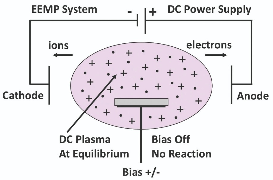
Figure 1. Electron-enhanced material processing begins by generating a room-temperature argon plasma, formed by the flow of a direct current between the cathode and anode. The bias signal is generated separately and is connected to the wafer stage.
Success in this arena requires a high-quality etching technology. It is critical to defining device features and ensuring optimal surfaces and interfaces, prior to growth, deposition or implantation of the next element of circuit design.Since the introduction of plasma etching in the 1970s, etching technologies have steadily advanced. The two most prominent are reactive-ion etching and atomic-layer etching. Both bombard the surface with ions – in one case, it’s reactive ions; and in the other, it’s argon ions. Neither option is ideal, because the ions that bombard the surface can damage the crystalline structure, which may be further impaired by exposure to elevated processing temperatures.
Etching with electrons
Addressing these conditions is an electron-enhanced material processing technology that we have developed at Velvetch, a start-up based in Pasadena, California, that has teamed with PVATepLa America to manufacture and support the systems. Our process is based on a fundamentally different etch mechanism, utilising a room-temperature DC plasma to produce wafer-scale waves of precisely controlled electrons. These electrons stimulate an excited-state etch reaction across the entire surface of the material.
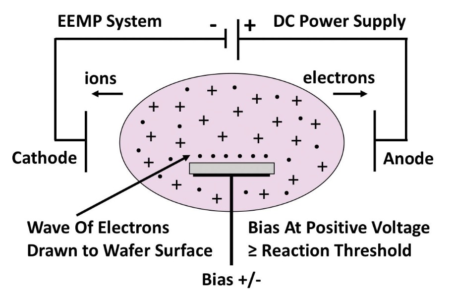
Figure 2. In an electron-enhanced material processing tool, a wave of precisely controlled electrons is drawn to a sample that is held on the wafer stage when the bias signal is driven positive to a voltage equal to or greater than the desired excited state reaction threshold.
With this approach, each excited state reaction involves a material-specific energy threshold. Each wave of electrons interacts with the surface, providing exactly the right amount of energy necessary to drive the desired reaction. Due to a direct quantum excitation of bonds on the wafer surface, etching takes place one atomic layer at a time. The anisotropic etch that results is accomplished with a high etch rate, absence of any ion bombardment damage, and the elimination of any exposure of the wafer to elevated temperatures. Additional merits of our etching technology are that it yields atomically smooth surfaces, and it preserves the stoichiometry of the material.Etching begins by mounting a wafer on a stage immersed in an equipotential, positive column of a DC plasma (see Figure 1). To maintain the plasma, a low-voltage DC current is directed through electrodes outside the wafer-stage zone. In the absence of an etch bias, electrons in the DC plasma equilibrate to the uniform plasma potential. The etch is initiated by applying a positive etch bias to the wafer stage. This draws down a dense wave of precisely controlled electrons to the surface of the wafer with an energy equal to the difference between the DC plasma potential and the voltage of the etch bias (see Figure 2).
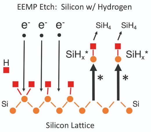
Figure 3. When using electron-enhanced material processing to etch silicon with hydrogen, the process begins with a wave of electrons arriving at the silicon lattice (see left side). After the reaction, excited state etch products depart the silicon lattice (see the right side).
One of the merits of using electrons rather than ions is that thanks to their far lower mass, they move downward almost instantaneously. While this takes place, the positive ions drift slowly upward. When each wafer-scale wave of electrons arrives on the wafer from above, this produces an excited-state chemical reaction between the etchant gas and the top layer of atoms.A simple, illustrative demonstration of how electron-enhanced material processing works, and its unique capabilities, is the etching of silicon with hydrogen (see Figure 3). During this process, neutral hydrogen atoms form a loosely bound corrosion layer with the dangling bonds of the top atomic layer of silicon. Note, however, that hydrogen does not etch silicon until the next wave of electrons arrives with the positive-going etch bias. At this point, electrons directly couple their energy into the electron orbitals of the silicon atoms, and partially reacted etch products are raised to an excited energy state. The top layer of the silicon atoms is then instantly released from the lattice, and excited-state etch products are repelled from the silicon surface.
During this reaction, three excited-state etch products result from the reaction of silicon and hydrogen: SiH1*, SiH2* and SiH3*. The predominant product is SiH2*, because the top layer of a silicon lattice tends to present two dangling bonds to the vacuum.
All three forms of excited-state etch product react with hydrogen in the room-temperature argon plasma. This generates a SiH4 etch product, which drops back down to the ground state as it is pumped away by the etch system. As the excited state reaction proceeds, the temperature of the silicon wafer rises by no more than a couple of degrees.
Swap hydrogen for chlorine and atomic layer etching still proceeds in the same manner. Excited etch products are now SiCl*, SiCl2* and SiCl3*, and SiCl4 is the final etch product (see Figure 4).
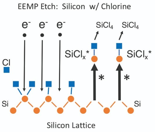
Figure 4. Etching silicon with chlorine via electron-enhanced material processing. A wave of electrons arrives at the silicon lattice (left side), and excited state etch products depart from this surface (right side).
Etching GaAs and GaNElectron-enhanced material processing of GaAs and GaN proceeds in the same manner as for silicon, except there are two excited-state chemistry reaction pathways for the etch products (see Figures 5 and 6). For GaAs, excited state etch products for gallium and arsenic are GaCl* and GaCl2*, and AsCl* and AsCl2*, respectively, and final neutral etch products are GaCl3 and AsCl3. Despite boiling points for GaCl3 and AsCl3 of 201°C and 130°C, respectively, the etch process can take place at less than 40°C because the excited-state etch products of GaAs instantly release from the wafer surface. By the time they finish reacting with chlorine to become final, neutral, etch products, they have already been pumped away.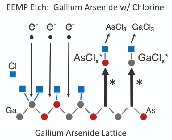
Figure 5. There are two excited-state reaction pathways for etching GaAs with chlorine by electron-enhanced material processing: one is for etching gallium with chlorine, and the other for etching arsenic with chlorine.
Using a chlorine etch, our results on GaAs are comparable to those on silicon, in terms of etch rate and atomic smoothness. During our tests, we inspected our epi-ready GaAs wafers prior to etching with a scanning electron microscope. Imaging the polished GaAs wafers revealed some minor striations, an artefact of the final polish provided by a chemical mechanical polishing process. After etching these wafers with our process, striations are absent in scanning electron microscopy images. Further evidence of the high-quality of our electron-enhanced material processing technique is provided by atomic force microscopy measurements. For the post-etched surface, root-mean square roughness is just 2 Å – that’s well below the GaAs lattice constant of 5.6 Å. To put it another way, our etching technology smooths the surface to within one atomic layer over a 4 µm2 scale.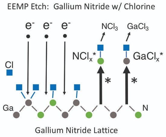
Figure 6. There are two excited state reaction pathways for the etching of GaN with chlorine by electron-enhanced material processing. The excited-state etch products for gallium are GaCl* and GaCl2*, and the excited-state etch products for nitrogen are NCl* and NCl2*. The final neutral etch products for GaN are GaCl3 and NCl3.
Another benefit of our electron-enhanced material processing technology, evident in our etching of GaAs wafers with chlorine, is that it faithfully preserves the stoichiometry of the crystal lattice. This is evident in the X-ray rocking curve of our etched wafer (see Figure 7), which has a near complete overlap with the curve produced by an unetched wafer.Using a standard plasma etch process gives a different result. When we applied plasma etching to a GaAs wafer – using a gentle reactive recipe with a mixture of SiCl4 and BCl3 as the reactant gases – raised shoulders appeared in an X-ray rocking curve. These features were not seen in the equivalent curve for an untouched GaAs wafer (see Figure 8), and prove that standard plasma etching alters the stoichiometry of the etched GaAs wafer, while it is retained with the electron-enhanced material process.
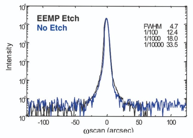
Figure 7. X-ray rocking curves provide a comparison of GaAs etched by electron-enhanced material processing (black) and unetched GaAs (blue). The two curves are almost identical, indicating etching did not alter the stoichiometry.
When we applied our electron-enhanced material processing technology to GaN-on-SiC wafers, it delivered equally impressive results. Using a chlorine etch recipe, we reduced the top surface of the GaN wafers from an as-received root-mean square surface roughness of between 8.5 Å and 10 Å to just 2.5 Å. To put the latter figure in perspective, GaN has a lattice constant of 5.2 Å, so with our etch we smoothed the GaN epilayer to within one atomic layer of atomic smoothness.We have also applied our chlorine etch technology to the contact areas of GaN-on-sapphire diodes, working in partnership with a team at the University of California, Santa Barbara. This study involved etching through the 40 nm GaN cap to open a contact pattern on the p-GaN surface of a p-n diode (see Figure 9), before depositing a metal contact on the exposed p-GaN surface. This diode, formed using a 3 minute contact etch, had a turn-on voltage of approximately 6 V. In comparison, controls produced by reactive-ion etching had turn-on voltages in the 10 V to 12 V range. We attribute the superior turn-on voltage to our damage-free, stoichiometry preserving etch technology.
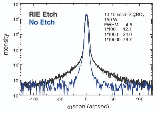
Figure 8. Compared to the X-ray rocking curve of unetched GaAs (blue), that subjected to reactive-ion etching (black) has elevated shoulders. This feature reveals that reactive-ion etching creates lattice damage to GaAs and alters its stoichiometry.
Stopping on a II-VIOne of the more difficult challenges encountered when etching compound semiconductors is the damage-free removal of the growth substrate from an epitaxial stack containing quantum wells. This is a problem that we have worked on through a collaboration with VerLASE Technologies.
Our efforts involved removing a GaAs substrate from the bottom of a II-VI device containing ZnSe quantum wells, ZnCdSe barriers, and ZnSe optical window caps surrounding the active region. We began by mounting the ZnSe top cap of the II-VI on a temporary glass plate, flipping over the assembly (see Figure 11) and etching the GaAs substrate.
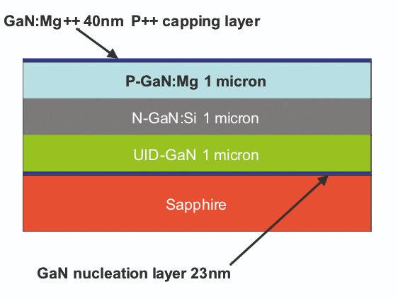
Figure 9. To make the contact to the p-GaN diode layer, etching is used to create an opening in the GaN p++ capping layer.
Previous efforts to remove the GaAs substrate with plasma etching had proved problematic, with ion bombardment generated by the plasma process damaging the ZnSe cap. Surface damage attenuated light entering the quantum well device, while deterioration of lattice quality diminished the Q factor of the quantum well, leading to a broadening of the spectral emission.
Thanks to the precision with which we control the electron energy during our etch, we were able to use our technology to remove the GaAs layer and make a hard stop on the ZnSe cap layer, without causing any damage. Employing a technique known as ‘special aperture plate’, we etched several test spots on the wafer. At every additional spot, we incrementally increased the electron energy, allowing us to characterize the etch threshold for the GaAs layer.
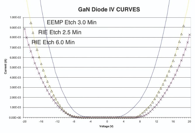
Figure 10. Current-voltage plots for GaN diodes, formed by etching the p-GaN contact, highlight the superiority of electron-enhanced material processing (blue trace) to reactive-ion etching (yellow triangles and pink crosses are for reactive-ion etching processes with a duration of 150 second and 6 minutes, respectively).
Based on our findings, we set the electron energy to the appropriate level, before performing several more etch runs to remove the GaAs substrate layer while coming to a hard stop on the ZnSe cap. This created several quantum well device spots. Thanks to the precise control of the electron energy, we could ‘over-etch’ the GaAs layer – that allowed us to completely clear away the last several atomic layers of GaAs, without damaging the ZnSe cap.Researchers at VerLASE have found that the ZnSe cap associated with the quantum well device spots is as optically smooth as the original surface. Spectral analysis verifies that no damage has been imparted to the cubic zincblende lattice structure of the ZnSe cap layer.
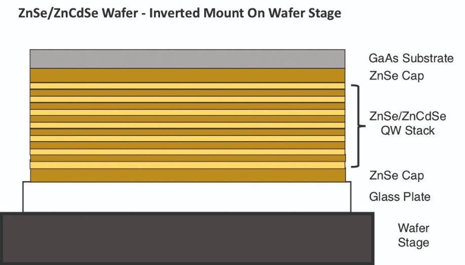
Figure 11. Electron-enhanced material processing enables damage-free removal of a GaAs growth substrate from an epistack containing a ZnSe/ZnCdSe quantum well device. To liberate the GaAs substrate, it is mounted to a glass plate, then inverted.
Our efforts show that our electron-enhanced material processing technology is capable of controlling excited-state surface chemistry reactions at a wafer scale. This opens up new possibilities for fabricating III-V, II-VI and quantum well devices that deliver the higher performance, higher output powers and higher efficiencies needed to meet the demands of rapidly growing applications for compound semiconductor devices. Our technology may also application in other markets, such as nano-materials and bio-compatible materials, where low temperature, damage-free etching and surface modification could be key attributes for novel device fabrication.


