
Compound Photonics opens MicroLED innovation centre
Arizona-based MiAC fab aims to accelerate time‐to‐market of sub 5 μm pixel monolithically integrated microLED displays
Compound Photonics US Corporation, a maker of compact microdisplay solutions for Augmented and Mixed Reality (AR/MR), has opened its MiAC (MicroLED Innovation Acceleration Center) in Chandler, Arizona.
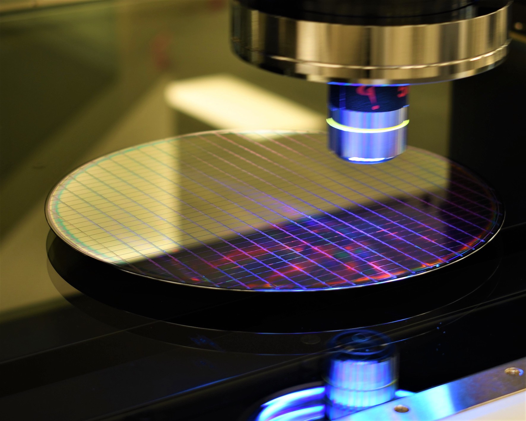
According to the company, out will be the world's first fab dedicated to accelerate the time‐to‐market of sub 5 μm pixel monolithically integrated microLED displays to meet the rising demand for mass market AR/MR and smart wearable devices.
Arizona Governor Doug Ducey commented: “Companies like Compound Photonics are strengthening Arizona’s reputation as the best place in the country to develop cutting‐edge technologies. Arizona is proud to be chosen as the home of this state‐of‐the‐art facility and we congratulate CP on their expansion.”
Arizona Commerce Authority President & CEO Sandra Watson said:“Arizona’s advanced manufacturing industry continues to grow rapidly thanks to investments from innovators like Compound Photonics. Skilled tech talent, a strong supply chain, and the best pro‐innovation environment in the nation continue to make our state the location of choice for next‐gen projects like the MiAC fab.”
Chandler Mayor Kevin Hartke stated: “It is very exciting to see companies in Chandler like Compound Photonics pushing the frontiers of augmented and mixed reality. We are delighted that CP is bringing more global resources to our city and contributing towards Chandler's high‐tech job growth."
Richard Jackson, CP’s Co‐CEO added: “Microdisplay has been a critical component that determines form factor, size, power consumption and optical performance of mainstream AR glasses. CP has been in the forefront of delivering a cutting edge of sub 3 micron pixel display drive technology & platform with a track record of bringing production‐worthy products to market. By aligning with our partners’ expertise, equipment and resources at MiAC, together we will accelerate microLED process advancement to be ready to scale for commercialisation.”
With over $20 million investment since 2018, the MiAC will facilitate a strong collaboration among CP and its industry partners in one high‐tech workspace. The approximately 15,000‐square‐foot, Class 100 clean room provides direct access to specialised fabrication and metrology equipment to facilitate advanced process.


