Moving Microscopy out of the lab with nanoLEDs

European researchers are developing a new generation of super resolution chip-sized optical microscopes using nanoLEDs
Optical microscopy is entering a new world, according to researchers from an EU-funded project called ChipScope. Future microscopes will be chip-sized and available in everyday life, not just in specialist laboratories. It might even become possible to detect SARS-CoV-2 and other viruses using a smartphone.
“This use of chip integrated nanoLEDs will revolutionise the way science and applications related to optical microscopy will be done in the future,” says Angel Dieguez, professor at the University of Barcelona, Spain. “It can be used to investigate extremely small structures such as viruses, DNA or living cells, almost anywhere and in real time.”
The resolution of conventional light microscopes, still standard equipment in laboratories, is limited by diffraction: they can’t resolve structural features smaller than about 200 nanometres. Until now, all technologies for going beyond this limit rely on complex setups, with bulky components and advanced laboratory infrastructure. They are not suitable for mobile research devices used in field or in remote areas.
The University of Barcelona is one of a number of partners in ChipScope, a project supported by the EU-programme FET (Future and Emerging Technologies) (now part of EIC Pathfinder) which is developing an array of nanoLEDs with individual pixel operation. LEDs smaller than the diffraction limit will be used as light sources for a microscope, which will be integrated on a chip. “This will lead to extreme miniaturisation and simplicity for super-resolution microscopy,” Dieguez explains.
The project’s members are universities and research centres as well as small and medium sized enterprises (SME). They intend to integrate the nanoLEDs into a real-time imaging device.
Dieguez explains: “In conventional optical microscopy, the area that needs to be analysed is illuminated simultaneously, collecting the light which is scattered from each point of the sample with the human eye or the sensor of a camera as a sensitive detector. Our idea, however, is based on a structured light source with tiny, individually addressable elements. The sample is put on top of this light source. Whenever single emitters are activated, the light propagation depends on the spatial structure of the sample.”
“This is very similar to shadow imaging in the macroscopic world. To obtain an image, the overall amount of light which is transmitted through the sample region is sensed by a detector, activating one light element at a time and thereby scanning across the sample space.”
The GaN-based nanoLEDs, which are the first with individually addressable pixels in the sub-micrometre range to become available on a commercial scale, are being developed at the Braunschweig University of Technology, Germany.
Dieguez’ own team in Barcelona constructed the light detectors: “We now have a prototype device to conduct further experiments. Other projects will be tasked with making a marketable microscope. I don’t have a time scale in mind, but I’m convinced that this will revolutionise the microscope market and the ways to do field research. With chips instead of lenses, the devices will be very mobile extremely cheap. They also can be integrated into existing tabletop systems.”
DNA chip fabrication and optogenetics
Joan Daniel Prades is also a professor at the University of Barcelona and coordinates SMILE (Scalable Structured Micro-Illumination Light Engines), which is using the outcomes of ChipScope. The researchers are developing microLED devices that can bring innovation in microscopy and other research fields such as DNA chip fabrication and optogenetics.
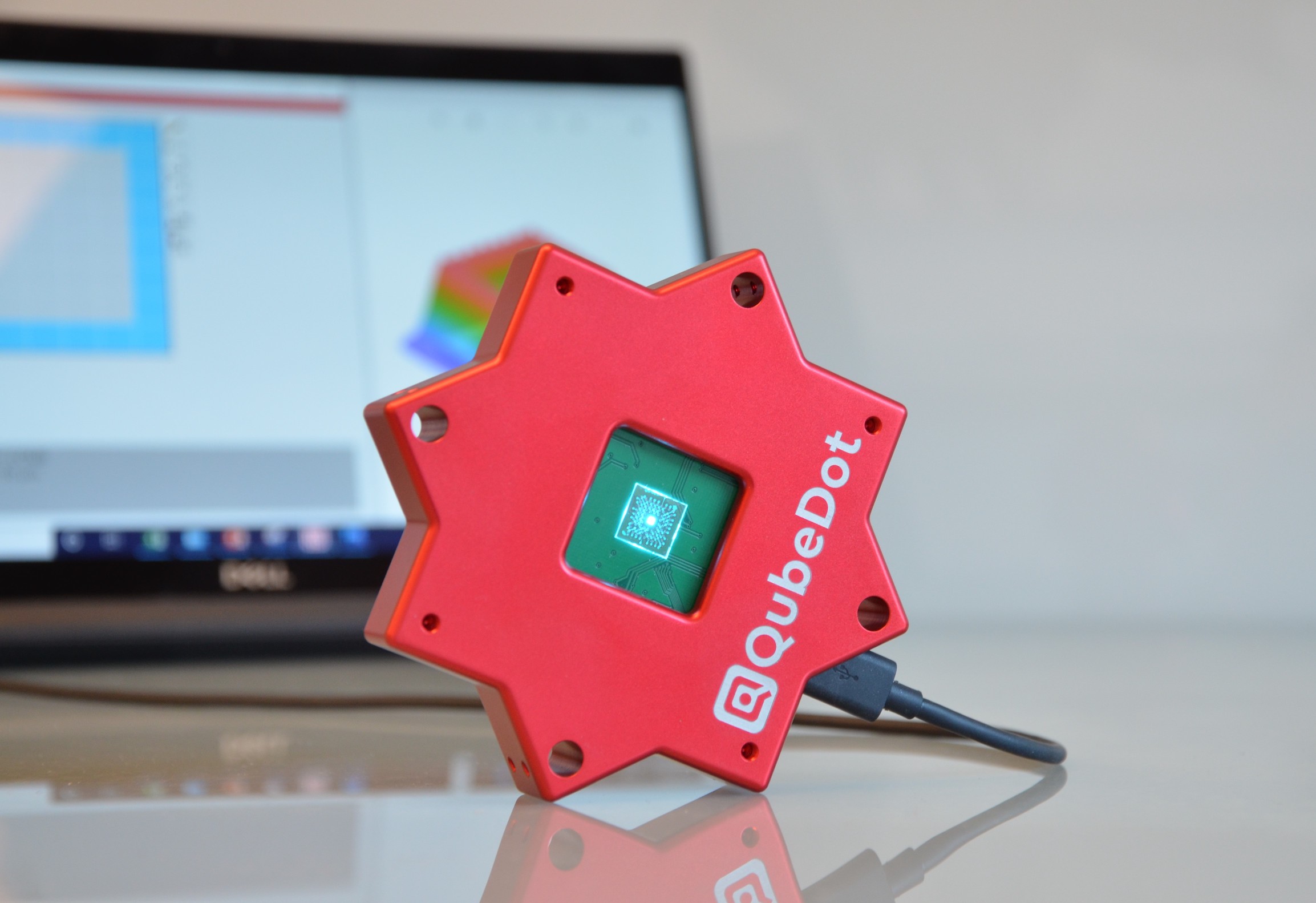
Particularly for optical microscopy, the researchers see possibilities to study the properties of large quantities of substances. “We try to combine holography and chip-based technology with microscopy to allow transparent cells to be visualised with classic cell culture plates. Today, we have a prototype that allows a resolution of 256 pixels per inch, which is available through our start-up partner QubeDot (Braunschweig, Germany). The project’s goal is to obtain 2,000 pixels.”
Another application is the fabrication of DNA biochips. Prades explains: “DNA chips or DNA microarrays are an important tool for gene expression analysis. These chips consist of a solid surface with a collection of single-stranded DNA fragments [which is the known sequence, ed. Note]. The DNA samples that need to be analysed [the unknown sequence, ed. Note] are fluorescently labelled and fixed onto the chip.” The complementary binding between the known and the unknown sequences is then analysed.
Using microarray technology, the researchers can get information on thousands of genes simultaneously with just a single DNA chip. “A similar application already exists with lasers. However, these produce DNA samples point by point, whereas DNA chips will perform this task by blocks, which means they work much faster,” Prades continues.
The project also aims at bringing innovation into optogenetics, which is a biological technique that uses light to activate of deactivate individual neurons or neuronal networks in the brain of living animals by shining light on them. Up to now, complex fibre optics systems are used to do this. “The time to generate a pixel and switch to the next one will be less than ten nanoseconds, at a full framerate of 1 MHz. So, the planned systems will encompass relevant existing restrictions regarding the maximal frequency of activation, minimum spot size and maximal power output. In addition, conventional microscopy systems are very costly and not readily available, leading to restrictions in the number of experiments to be performed per time, which limits scientific progress.”
Photolithography is another field of application: “Manipulation technologies enabled by large computing capacity allow high replication throughputs as demanded for in industrial micro-patterning.”
The project is one of the EIC Transition to Innovation Activities, which aim at bringing innovative FET technologies to a level of development for business creation. “An end-user board, with experts from various branches – multinationals, SMEs and interdisciplinary research institutes – will perform tests and validations for quickly increasing markets with the prototypes we are going to make available in five pilot applications,” Prades concludes.


