
Perovskite tandem on threshold of 30 percent efficiency
HZB's current world record tandem solar cell provided stable performance for 300 hours - even without encapsulation
Early in 2020, a team headed by Steve Albrecht at HZB broke the previous world record for tandem solar cells made of perovskite and silicon (28.0 percent, Oxford PV), setting a new world record of 29.15 percent. Now, the results have been published in the journal Science with a detailed explanation of the fabrication process and underlying physics.
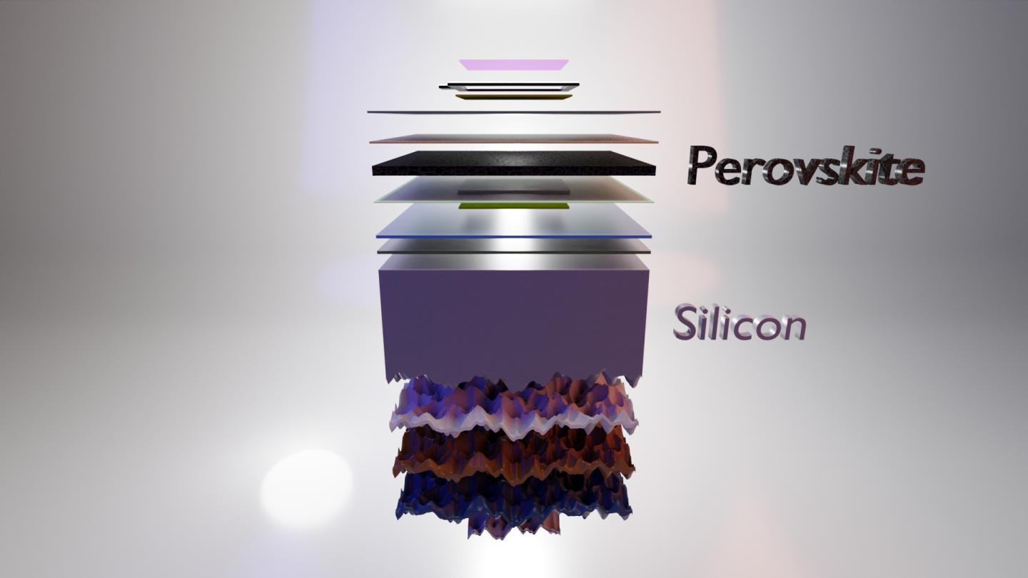
"29.15 percent efficiency is not only the record for this technology but is at the very top of the entire Emerging PV category in the NREL chart", says Eike Köhnen, PhD student on Albrecht's team and shared first author of the study. In addition, the new perovskite/silicon tandem cell is characterised by consistent performance during more than 300 hours under continuous exposure to air and simulated sunlight without being protected by encapsulation. The team utilised a complex perovskite composition with a 1.68 eV band gap and focussed on optimising the substrate interface.
With partners from Lithuania (the group of Vytautas Getautis) they developed an intermediate layer of organic molecules that arrange themselves autonomously into a self-assembled monolayer (SAM). It consisted of a novel carbazole-based molecule with methyl group substitution (Me-4PACz). This SAM was applied to the electrode and facilitated the flow of the electrical charge carriers. "We first prepared the perfect bed, so to speak, on which the perovskite lays on", says Amran Al-Ashouri, who is also a member of Albrecht's team and shared first author of the study.
The researchers then used a range of complementary investigation methods to analyse the different processes at the interfaces between perovskite, SAM, and the electrode: "In particular, we optimised what is called the fill factor, which is influenced by how many charge carriers are lost on their way out of the perovskite top cell", explains Al-Ashouri. While the electrons flow off in the direction of sunlight through the C60 layer, the 'holes' move in the opposite direction through the SAM layer into the electrode. "However, we observed that the extraction of holes is much slower than electron extraction, which limited the fill factor", says Al-Ashouri. However, the new SAM layer considerably accelerated the hole transport and thus simultaneously contributes to improved stability of the perovskite layer.
Through a combination of photoluminescence spectroscopy, modelling, electrical characterisation, and terahertz conductivity measurements, it was possible to distinguish the various processes at the interface of the perovskite material and to determine the origin of significant losses.
Many partners were involved in the project, including Kaunas University of Technology/Lithuania, University of Potsdam, University of Ljubljana/Slovenia, University of Sheffield/UK, as well as the Physikalisch-Technische Bundesanstalt (PTB), HTW Berlin, and the Technische Universität Berlin, where Albrecht holds a junior professorship. The work on the individual perovskite and silicon cells took place in the HZB labs HySPRINT and PVcomB, respectively.
"Each partner brought their own special expertise to the project, so we were able to achieve this breakthrough together", says Albrecht. The maximum possible efficiency is already within reach: the researchers analysed the two cells individually and calculated a maximum possible efficiency of 32.4 percent for this design. "We can certainly achieve over 30 percent", says Albrecht.
'Over 29 percent- efficient Monolithic Perovskite/Silicon Tandem Solar Cell Enabled by Enhanced Hole Extraction'; Science 11th December 2020


