

Scrutinising GaN HEMTs by quantitative cathodoluminescence
Quantitative cathodoluminescence aids development and production of GaN HEMTs by delivering non destructive measurements for threading dislocations, composition, and doping
BY MATTHEW DAVIES AND CHRISTIAN MONACHON FROM ATTOLIGHT
COMPOUND SEMICONDUCTORS share many of silicon’s characteristics. However, there are some notable differences, causing some characterisation techniques for silicon to fail to provide accurate information for compound semiconductors. This state of affairs is most evident with GaN. To ensure competitive pricing, GaN transistors and LEDs are grown on foreign substrates, giving rise to a very high defect density in the epilayers, a situation never found in silicon devices.
Helping to characterise various compound semiconductor devices, including those made from GaN, is a non-destructive technique known as quantitative cathodoluminescence spectroscopy. This is being trailblazed by our team at Attolight of Lausanne, Switzerland, which has launched tools that support this form of metrology.
 Previously, our team reported how quantitative cathodoluminescence spectroscopy can assist manufacturers of solar cells, lighting, and display technologies (see, for example, Cathodoluminescence for high-volume manufacturing, from the July 2018 edition of Compound Semiconductor). Here we consider how this technique can monitor the quality of the heterostructure of another device, the GaN-on-silicon HEMT (if you are not familiar with this device, take a look at the box “The basics of the GaN HEMT”).
For this class of transistor, quantitative cathodoluminescence spectroscopy allows engineers to optimise end-of-line yield by focusing on three key metrics: the threading dislocation density; the aluminium content of the AlGaN layer above the channel; and the magnesium doping content of the p-type GaN gate, key to the realisation of a normally-off HEMT.
To ensure optimal process chain management, engineers need to draw on rapid non-destructive feedback from metrology tools at every step of the process chain. This holds true for pilot lines, and for those found in dedicated research and development facilities and high-volume fabs. For those working in research and development, faster feedback accelerates development, while improving its efficiency and trimming costs. In the high-volume fab, faster non-destructive feedback reduces work-in-progress and aids rapid process steering – in an ideal case, the effective work-in-progress is zero for a given process step. This is possible when feedback from a metrology tool is available within the downtime of a process tool between subsequent processes, a situation that occurs, for example, when cleaning an epi-reactor.
Our Säntis platform – for use after the growth of the epiwafers – offers rapid, reliable, non-destructive feedback of various metrics previously only accessible via destructive, time-consuming methods. Armed with this new, high-resolution eye on the epiwafers, fab managers and their engineers are well-positioned to make critical processing decisions. This includes deciding whether certain wafers should proceed to front-end processing, and whether there is a need to tweak the growth recipe, based on immediate feedback on key performance indicators.
In the remainder of this article we describe studies of GaN HEMTs using our Säntis 300 full-wafer quantitative cathodoluminescence platform. These investigations, which include proprietary measurement and analysis methods specifically developed for power HEMTs, represent the current state of development of our technologies for epi process control in GaN manufacturing.
Determining dislocations…
Dragging down the performance of GaN HEMTs are threading dislocations. If they intersect the channel formed by the two-dimensional electron gas, or connect the substrate to the gate contact, they can cause device leakage currents [2] and potentially impair long-term device robustness. Developers of GaN HEMTs have devised several solutions for cutting the leakage current through these channels. However, those working in this field are still to grasp a full understanding of this issue – they don’t have a complete picture for what allows current leakage via these dislocations, or how to effectively control leakage, and they don’t know the impact of dislocations on device performance and robustness. Consequently, there is a need to analyse threading dislocations in the epilayers, as this will shed more light on this issue and help to control the process, leading to better devices.
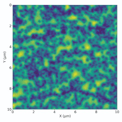
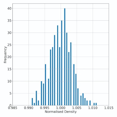
Figure 1. (a). A cathodoluminescence image with threading dislocations identified by the highlighted Attolight image reconstruction solution. (b) Histogram of normalised threading dislocation densities, recorded over several hundred iterations of the image reconstruction algorithm.
As cathodoluminescence has been around for decades, it is often assumed that counting threading dislocations by this technique is trivial. But it’s not: it is far more complex than it would first appear to ensure reliable determination of the threading dislocation density to a standard that meets the expectations of process control metrology.However, quantitative cathodoluminescence is incredibly insightful, combining simple counting of threading dislocations and determining their density with many new metrics. They include the local spatial distribution of threading dislocations; their geometric order and size; and the ability to discriminate between this imperfection and other structural defects, such as V-shaped pits. Thanks to this broad range of capabilities, quantitative cathodoluminescence spectroscopy is a very powerful tool for supporting the development and production of the GaN HEMT.
One technique with the potential to help quantitative cathodoluminescence is machine vision, which has improved in recent years, leading to widespread implementation in many industries. However, there are pitfalls when applying machine vision to small, densely packed features, such as the clusters of threading dislocations found in the epilayers of GaN-on-silicon HEMTs. In these heterostructures, where on average there are around ten threading dislocations per square micron, traditional feature-detection algorithms can suffer from a drop in accuracy.
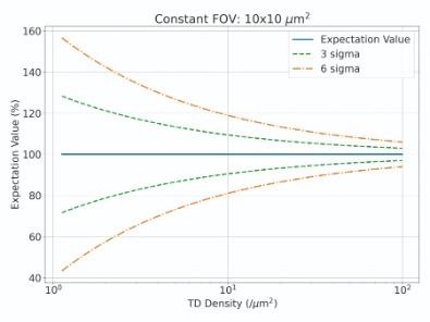
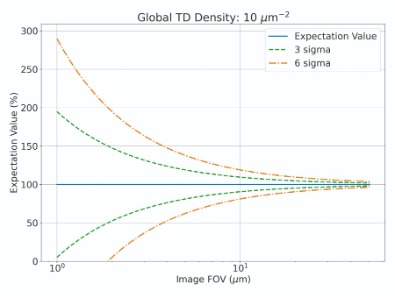
Figure 2. (a) Representative uncertainty (expressed as a percentage of the expectation value) for varying threading dislocation densities when considering a constant image area (FOV) in a single 10 x 10 μm2 image. (b) Representative uncertainty (expressed as percentage of the expectation value) for a constant threading dislocation density of 1 x 109 cm-2, evaluated for a single image with a varying FOV.
We have addressed this weakness with an innovative image reconstruction method that draws on the results of Monte-Carlo and numerical simulations, and material-specific knowledge and assumptions. After investigating hundreds of iterations across different images, we determined a reconstruction reproducibility, evaluated in terms of 3 sigma, of ±1.05 percent (see Figure 1). In addition, our technology resolves up to 40 percent more defects than a benchmark feature-detection solution.If threading dislocation imaging by quantitative cathodoluminescence is to be employed into process control its capabilities must be more than just accurate counting of these defects in a single image. It may appear that to maximise precision of detection, engineers should record fewer higher-resolution images, each with fewer features. But this can fail to consider both the accuracy and the management of sampling error. This is critical to allowing quantitative cathodoluminescence to play an important role in process control.
As illustrated in Figure 2, when smaller images are used to determine the threading dislocation density, there are fewer features present – and the image is more susceptible to random statistical fluctuation. While an individual image can provide a more precise detection of threading dislocations, in certain circumstances the sampling error overrides this gain, resulting in an inferior accuracy for the result.
Consider, for example, a single image with a small field of view. This can result in an extremely large range of possible values due to random statistical fluctuation, an effect exacerbated by lower threading dislocation densities. In an extreme case, when imaging a sample with a defect density of 1 x 109 cm-2 – this equates to an average of ten defects for every square micron – there is a small but non-zero probability of finding no defects in a single 2 x 2 μm2 field of view (this is illustrated in Figure 1 (b)).
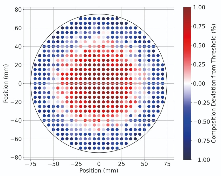
Figure 3. The Säntis 300 platform is capable of producing a wafer map of the aluminium composition of a buried AlGaN layer in a GaN HEMT structure (simulated data).
The solution is to combine a high sampling rate with an optimised field-of-view. Note, however, that it is not possible to process images with an infinitely large field-of-view with high precision, despite the apparent benefits that this would have on minimising sampling error. To realise sampling rates that ensure sufficient repeatability and reproducibility of process control metrology tools, there needs to be excellent, reliable automation, and repeatability of the detection algorithm. We offer this by combining: the automation of the Säntis 300 platform, with due consideration of sampling error and repeatability; with an innovative approach, employing a proprietary image reconstruction method to detect features.
…and epilayer compositions
Situated at the heart of every HEMT, whether it is normally-on or normally-off, is a layer of AlGaN that is integral to the formation of the two-dimensional electron gas channel. By carefully controlling the AlGaN growth, engineers can set the electron gas concentration and ultimately determine key characteristics, such as the threshold voltage and
the on-state series resistance.
The growth of the heterostructure for the GaN HEMT is never perfect. Due to epitaxial reactor design, substrate bow, and the kinetics of the growth process, there are radial wafer-level dependences associated with epilayer composition and thickness (see Figure 3). The variations they produce on critical layers – in the case of HEMTs, the AlGaN layer; and in LEDs, the active region – drive down wafer-level homogeneity and device yield. While metrology and monitoring of critical epilayers can’t eradicate this, they do play a crucial role in maximising homogeneity and manufacturing yield.
A very widely adopted, quick approach for determining the composition of epilayers involves measuring the peak of the photoluminescence. However, this is not applicable to all epitaxial structures, including buried AlGaN layers surrounded by GaN cladding. When AlGaN is buried, its energetic state relative to that of the neighbouring GaN layers results in an extremely low emission rate under optical excitation. Compounding matters, the excitation process for the AlGaN layer is inefficient, especially as the layers above it absorb most, if not all, of the incident laser light. Due to these two factors, it is impossible to measure the photoluminescence from a buried AlGaN layer.
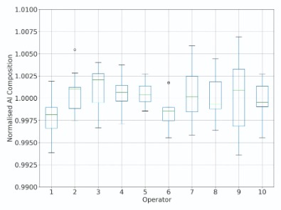
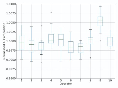
Figure 4. Representative results of a nested Gage reproducibility and reliability study on the determination of aluminium composition in the AlGaN layer of: (a) a full normally-off GaN HEMT structure (buried layer); and (b), the equivalent HEMT structure with the p-type GaN cap removed (surface layer).
Options for overcoming this problem are to either interrupt the growth after deposition of AlGaN, or to expose AlGaN by etching the material above it. Neither are ideal, being destructive processes. Regardless of whether the wafer is etched, or the growth interrupted, material used for photoluminescence measurements cannot be processed into devices. Another limitation is that this approach involves an indirect feedback loop, because measurements are performed on sister wafers.Our approach offers a superior alternative, adjusting the electron-beam penetration depth to more efficiently and precisely excite the buried AlGaN layer. We have proven the accuracy and reproducibility of our technique by using a nested Gage study to compare equivalent wafers with and without a top p-type GaN layer (see Figure 4). This study shows a strong measurement reproducibility, with standard deviations below ± 0.25 percent [of normalised value], based on over 100 repeat measurements. When assuming a 14 percent specification limit (target ±7 percent), we record a Gage variance below 10 percent for each sample.
Doping control
In normally-off GaN HEMTs magnesium doping influences various device characteristics, including robustness, off-state leakage and threshold voltage. The pioneers of GaN devoted much effort to developing a process for realising magnesium doping, with success in the 1990s allowing GaN to overtake ZnSe and become the best material for making blue and green LEDs and lasers. In the decades that have followed, those working on GaN have made a great deal of progress in understanding magnesium doping, with the self-compensation mechanism investigated and discussed in the research community [5]. Yet despite these advances, magnesium doping in the GaN HEMT still presents complications. Issues include enhanced leakage paths, stemming from an interplay between magnesium acceptors and threading dislocations [6].
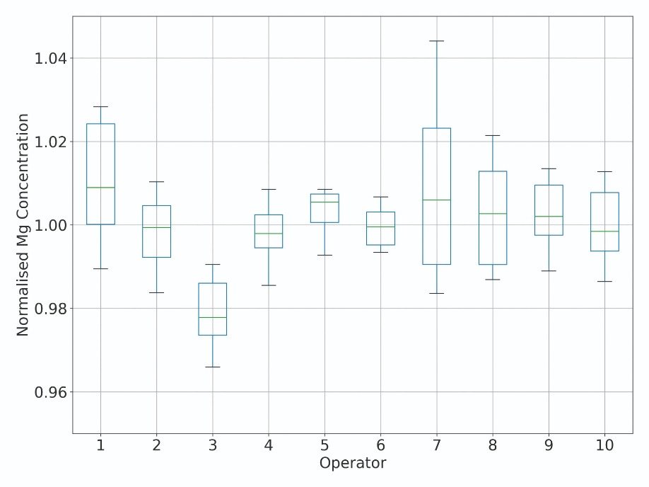
Figure 5. Representative results of a nested Gage reproducibility and reliability study on the determination of the magnesium concentration in the p-type GaN layer of a full normally-off GaN HEMT structure.
The traditional technique for measuring magnesium-doping in GaN is Secondary Ion Mass Spectrometry (SIMS). Used alongside Hall effect measurements, it allows engineers to uncover the ratio of incorporated magnesium to electrically active magnesium. Unfortunately, SIMS and Hall effect measurements are both destructive, with the former sometimes even requiring the shipment of a sample to a specialist lab.However, long waiting times for both on- and off-site SIMS measurements no longer need to hamper progress, thanks to our proprietary technique for determining the magnesium concentration by quantitative cathodoluminescence. Our approach, based on detailed spectroscopic analyses, draws on a deep understanding of electron-matter interactions and the cathodoluminescence technique, as well as material-specific expertise.
To prove the capability of quantitative cathodoluminescence spectroscopy for determining magnesium doping, we have compared the results it produces to those provided by SIMS. Measurements on multiple samples yields a root-mean-square error of 3.8 percent for the derived relationship between magnesium concentrations determined by SIMS and by quantitative cathodoluminescence. To determine the repeatability of our technique, we have carried out a nested Gage reproducibility and reliability study (see Figure 5). This investigation uncovered good reproducibility, with a standard deviation below ± 1 percent over 100 repeat measurements, when assuming a 60 percent specification limit (target ± 30 percent) and a Gage variance below 10 percent.
Three virtues
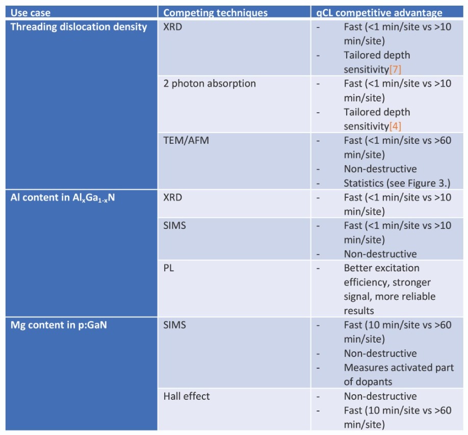
One of the great virtues of our approach is that it is non-destructive. This prevents wafers from being periodically sacrificed to determine a property – a particularly welcome asset for determining the magnesium content in GaN HEMTs, as all alternative techniques are destructive. The two other prominent virtues are that this technique is comparatively fast, enabling acquisition from dozens of sites per wafer, and therefore giving a sense of the homogeneity of the properties; and the approach has versatility, providing measurements of threading dislocation density, AlGaN composition and magnesium-doping levels. Although it takes time to move between samples, due to the need to exchange wafers under vacuum, fabs that invest in this tool save space and reduce complexity of their feedback cycle (all these benefits are highlighted in Table 1, which also outlines the pros and cons of other techniques).
Thanks to the virtues of the Säntis 300 platform, it is ideal for process control, providing non-destructive feedback in research and development labs and production fabs. By offering insights not available by other techniques, alongside faster feedback on existing metrics, it drives faster, more efficient development cycles in the lab, and trims work-in-progress in production cycles.
Alternative techniques for analysing GaN HEMT epiwafers highlight the advantage of the Attolight solution.
At the heart of the junction-gated, normally off HEMT [1] is a two-dimensional electron gas (2DEG), formed at the interface between the large band gap AlxGa1-xN (with x typically 10-20 percent) and regular GaN. To ensure normally-off operation, a p-type doped GaN layer is inserted between AlGaN and the gate contact.
For devices with this design, performance is impacted significantly by the:
Dislocation density. Dislocations are ultimately linked to leakage current [2]Magnesium concentration in p-type GaN. This affects the Fermi level of GaN underneath the gate, and ultimately the blocking power of the deviceAluminium concentration in AlGaN. This affects directly the 2DEG concentration [3]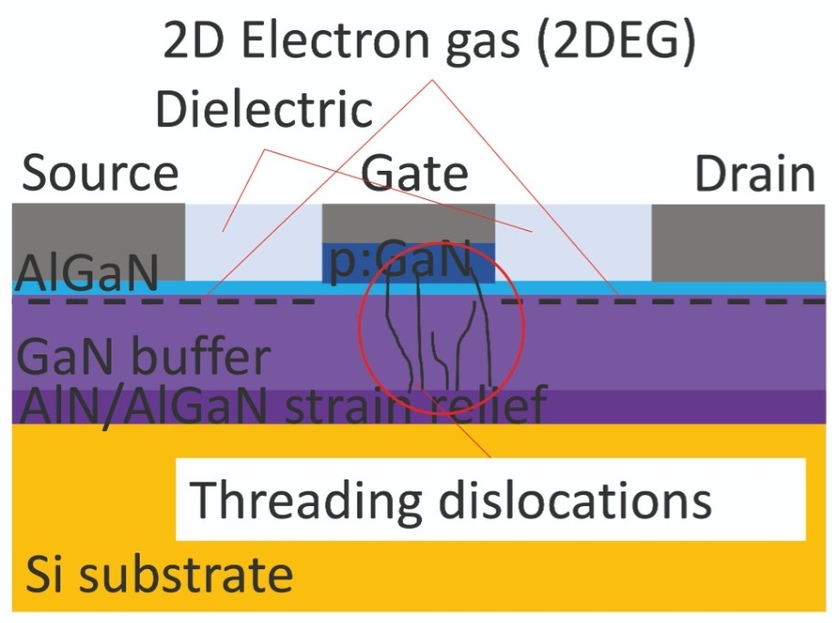
This is the general design of the junction-gated, normally-off HEMT, typically used for power-conversion applications. Threading dislocations are present in the entire sample. This sketch just indicates their presence and direction, especially under the gate, where they have potentially the largest impact.
[1] M. Meneghini et al., Power GaN Devices: Materials, Applications and Reliability. Springer Nature, 2017.
[2] S. Usami et al. Appl. Phys. Lett. 112 182106 (2018)
[3] Y. Ohmaki et al. Jpn. J. Appl. Phys. 45 L1168–L1170 (2006)
[4] I. Rossetto, et al. Microelectronics Reliability 76-77 298 (2017)
[5] A. Klump et al. J. Appl. Phys. 127 045702 (2020)
[6] J. Chen et al. Appl. Phys. Express 12 051010 (2019)
[7] V. Yon et al. Phys. Status Solidi 257 1900579 (2020)


