

Enhancing silicon photonics with III-Vs and barium titanate

Heterogeneous co-integration of barium titanate and III-V semiconductors on a silicon photonics platform enables efficient optical transceivers and novel neuromorphic devices
BY PASCAL STARK AND BERT JAN OFFREIN FROM IBM RESEARCH EUROPE AND STEFAN ABEL FROM LUMIPHASE AG
RECENTLY GLOBAL DATA TRAFFIC has been increasing at a compound annual growth rate of more than 25 percent. Due to this exponential rise, worldwide data traffic is tipped to reach 400 Exabytes per month in 2022. To cope with this hike in growth, which shows no sign of slowing, there needs to be a rapid scale-up in data transmission capacity and speed.
The lion’s share of the traffic occurs within datacentres, where data is routed through optical fibres over distances from a few metres to a few kilometres. Inserted at the interfaces between optical fibres and the electronic domain, involving computing and routing units, are high-speed optical transceivers (see Figure 1) – they are the most critical element in optical communication links.
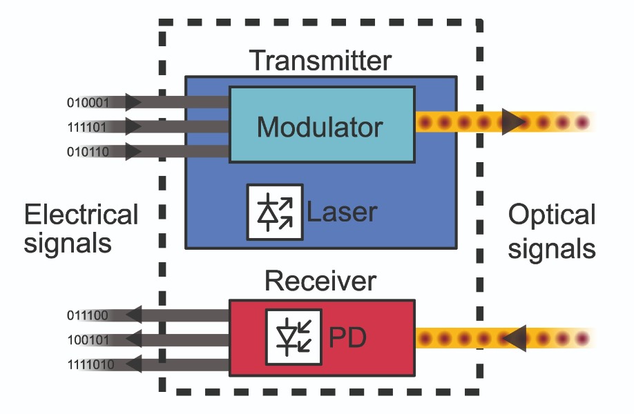
Figure 1. An optical transceiver provides an interface between electrical and optical communication channels. The transmitter converts electrical signals into optical signals. Vice-verse, the receiver is used to convert optical signals into electrical signals.
There are two parts to the optical transceiver: the transmitter and the receiver. The transmitter contains a high-speed electro-optical modulator, which encodes input signals onto an optical carrier by a continuous-wave laser diode. After encoding, the optical signal is transmitted over an optical fibre. When the optical signals reach the transceiver, they are converted from the optical domain to the electrical domain with a photodetector.Our team at IBM Research Europe has been pioneering a platform that paves the way to compact, high-bandwidth, power-efficient optical transceivers. At the heart of our technology is the co-integration of barium titanate (BTO), selected for its extremely strong electro-optic switching properties, with ultra-thin III-V technology, which provides a gain material for light emission, on a single silicon photonics platform. Lumiphase further develops such efficient switching products based on BTO photonic technology for commercial exploitation.
Here we detail how we integrate these different functional materials onto a silicon photonics platform. To fully unleash the functionality of all the layers, we have taken much care to ensure that we transfer light with low loss between different photonic layers. Efforts have also been directed at developing devices for potential applications such as optical transceivers and novel neuromorphic photonic architectures.
Silicon photonics: power and flexibility
The foundation for our work is silicon photonics. It offers efficient routing, manipulation, detection and modulation of light at telecommunication wavelengths, which span the range 1.3 μm to 1.55 μm. Today, silicon photonics is a mature photonic integrated circuit (PIC) technology, suitable for high-volume, low-cost production in CMOS foundries. Most commercial platforms are limited to the integration of PICs with optical components, such as waveguides, modulators and detectors, but also approaches to combine electronic and photonic integrated circuits (EPICs) are being developed. These approaches bring on-board electronic circuits, such as drivers, amplifiers, or control electronics, monolithically co-integrated with photonic components. Our technology is compatible with both PIC and EPIC platforms.
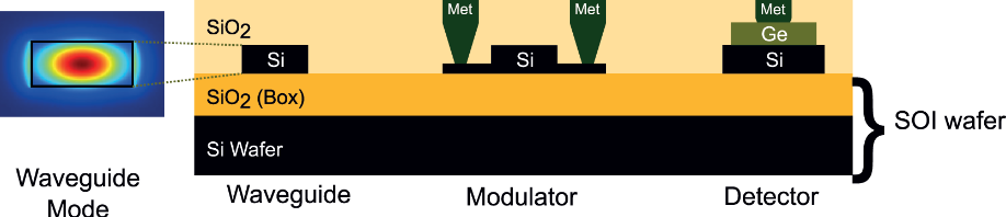
Figure 2. A silicon photonics platform with a waveguide, electro-optic modulator and germanium photodetector. Devices are fabricated on a silicon-on-insulator wafer (SOI). The waveguide mode shows the electric field intensity (red depicts high intensity, blue is for low intensity) in the waveguide (black box).
Silicon photonics is based on guiding light in silicon waveguides clad by SiO2. Manufacturing this technology in state-of-the-art processing facilities enables the production of waveguides with propagation losses below 1 dB/cm. Due to the high refractive index contrast between silicon and its native oxide, light is well confined in the waveguides, enabling the realisation of low-loss bends with radii below 10 μm. In addition to waveguides, there are many other passive building blocks in silicon photonic circuits, including: splitters and combiners; low-loss waveguide crossings; tapers; reflectors, which may be based on Bragg gratings; and Echelle gratings. Thanks to many years of research and development, various structures have been established, including passive filters that provide wavelength multiplexing and demultiplexing on photonic chips.It is also possible to produce some active components with silicon photonics. One example is the electro-optic modulators based on the plasma dispersion effect in silicon. Injecting or depleting carriers creates an electrically induced change in the refractive index. Instead of solely changing the real part of the refractive index, there is also a shift in the imaginary part, due to the plasma dispersion effect. As designers of advanced modulators do not welcome this change in absorption, it must be avoided to boost the performance of future generations of silicon photonic modulators.
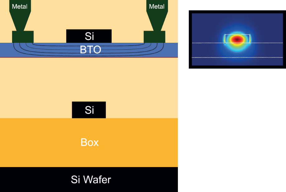
Figure 3. Cross section of a hybrid BTO/silicon device integrated on a silicon photonics platform. The refractive index of the BTO film (blue layer) can be tuned by applying an electric field (dotted lines). The inset shows the electrical field intensity of the optical mode in a hybrid silicon/BTO device. A large fraction of the optical power overlaps with the barium titanate film.
Two of the biggest drawbacks of silicon are that it cannot emit light; and that it is transparent at telecommunication wavelengths, making it unsuitable for efficient high-speed photodetectors. To equip circuits with these functionalities, direct-bandgap materials such as III-Vs are co-integrated with silicon. The most common approach for light detection is to add germanium, integrating this on silicon waveguides used for advanced photodetection. Far more challenging is the monolithic integration of the light source.Roles for barium titanate and III-Vs
A novel material for improving the performance of silicon photonics is the ferroelectric oxide barium titanate (BTO). It is blessed with one of the largest known Pockels coefficients – this means that it produces one of the most significant changes in refractive index upon application of an electric field. Additional merits of the Pockels effect in BTO are that the refractive index changes are ultra-fast, its static power consumption is extremely low, and it tunes purely the real part of the refractive index, without any absorption.
Exploiting all these strengths enables the construction of ultra-small, energy-efficient, fast modulators, optical switches, and tuning elements, operating by modulating the phase of an optical wave but not its amplitude. Note that there is no Pockels effect in silicon and realizing these functions directly in silicon through the plasma dispersion effect leads to much less favourable properties.
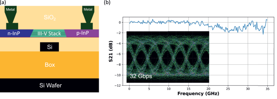
Figure 4. (a) Ultra-thin, CMOS compatible III-V integration on a silicon photonics platform. (b) Frequency response of a III-V photodetector. The inset shows an eye-diagram of the detector operated at 32 Gbit/s (NRZ signal) without using digital signal processing.
We integrate BTO by loading large silicon-on-insulator (SOI) substrates into an MBE chamber and epitaxially growing a thin film of this oxide. Subsequent low-temperature molecular wafer-bonding allows us to transfer the BTO films to a silicon photonics wafer. By limiting the thermal budget, we ensure that the integration of BTO is compatible with CMOS foundry processes, enabling co-integration with CMOS circuits. That is a major asset for high-speed applications, because monolithic co-integration limits unwanted capacitive effects.The next step in the fabrication process involves the etching of silicon waveguides into the silicon film on top of the BTO to create hybrid silicon/BTO devices (see Figure 3). The etched silicon waveguide guides the light, while a large fraction of the optical power overlaps with the underlying BTO film. Using this architecture, we have constructed Mach-Zehnder interferometers that offer efficient modulation and provide an excellent value for the figure of merit known as VπL– it is 0.2 Vcm, which is about one order of magnitude smaller than a typical silicon photonic modulator based on the plasma dispersion effect. As BTO modulators are field driven, they can also be used as low-loss switches, requiring a switching power of only about 100 nW.
As regular readers of this magazine know, III-Vs have been used for several decades to make high-performance lasers, as well as excellent photodetectors with bandwidths reaching more than 100 GHz. One option for integrating III-Vs with silicon is to employ the wafer bonding technique used to incorporate BTO films. However, today’s III-V stacks are often relatively thick, making them incompatible with the CMOS/silicon photonics process.
To use wafer bonding, III-Vs would have to be integrated on a CMOS/silicon photonics wafer in a dedicated fabrication line after completion of CMOS/silicon photonics processing. This effectively rules out direct co-integration with CMOS circuits.
To overcome this limitation we have been exploring the use of an ultra-thin hybrid III-V platform that is fully CMOS compatible. This approach involves lateral injection or collection of carriers in and out of the multi-quantum-well stack. Using ultra-thin stacks, we have built III-V photodetectors with a large bandwidth on a silicon photonics wafer (see Figure 4).
Creating co-integration
Each of the materials that we use has its particular strengths. Silicon holds the key to low-cost photonic circuits, BTO brings efficient modulation, and III-Vs offer efficient light emission and detection. To bring them all together in a single photonics platform we begin by fabricating a silicon photonic wafer with a planarized top surface, before transferring a single-crystal BTO layer onto the planarized surface and defining waveguides. Final steps involve bonding a III-V photonic layer, and subsequent processing to create active/passive devices (see Figure 5 for details).
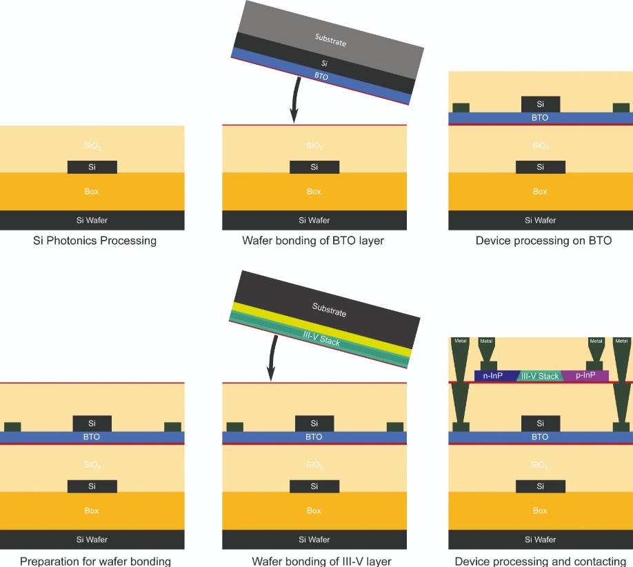
Figure 5. Co-integration of BTO/silicon and III-V technology on a silicon photonics wafer involves the following steps: (1) Processing a silicon photonics wafer and depositing a thin SiO2 layer on it. Preparing the SiO2 surface for molecular wafer bonding by chemical mechanical polishing (CMP). (2) Using molecular wafer bonding to integrate a BTO/silicon film on top of the silicon photonics wafer. (3) Defining devices on the BTO/silicon layer. (4) As in step 2, depositing a thin SiO2 layer and preparing its surface for molecular wafer bonding. (5) Using molecular wafer bonding to integrate a III-V layer on top of the stack. (6) Processing devices in the III-V layer and contacting devices in both co-integrated layers.
To leverage the benefits from all three classes of material, we use waveguide tapers to ensure a low optical loss when transferring light between the layers. The efficiency of these tapers is enhanced by employing an inverse direction on neighbouring layers. For example, to couple light from the silicon photonics layer to the BTO/silicon layer, we slowly decrease the width of the silicon photonics waveguide (taper down) while increasing the width of the BTO/silicon waveguide width (taper up).Reducing the silicon waveguide width leads to a decrease in the effective optical mode index and an increase in the mode size along the waveguide taper. This goes hand-in-hand with increasing the width of the BTO/silicon waveguide, which increases the effective mode index in the BTO/silicon waveguide.
As both waveguides are separated by only a thin SiO2 cladding, there is a small overlap between the silicon and BTO/silicon modes. This overlap propels the optical mode towards the region where the effective mode index is the largest. Consequently, the mode in the silicon waveguide is first converted into a hybrid mode propagating in both the silicon and BTO/silicon waveguides, prior to full transfer to the BTO/silicon layer. This process is incredibly efficient, allowing nearly 100 percent of the light to be transferred from the lower to the upper layer.
We have formed co-integrated structures by combining silicon photonic devices, formed on a 220 nm-thick layer of silicon sitting on 2 μm-thick buried oxide, with a BTO/silicon stack containing 100 nm-thick BTO and an intrinsic 250 nm-thick InP layer. Our entity features passive photonic elements on all photonic layers, demonstrating the simple building blocks of our concept. If we were to include active components, they would be realised with a similar process flow.
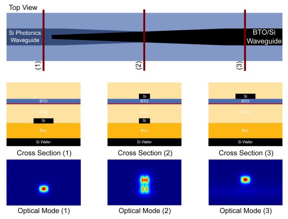
Figure 6. Inverse tapers on consecutive layers couple light between the layers. Shown here is a top view and corresponding cross sections and optical modes along a coupler between silicon and BTO/silicon. The mode is first guided in the silicon photonics waveguide. In the tapered section the mode converts into a hybrid mode, before it transfers to the BTO/silicon waveguide.
Within this structure, a low-loss intrinsic InP layer provides the III-V material stack. InP could act as a potential seed layer for subsequent III-V growth steps required for active III-V devices. This demonstrator, made using the process steps described previously, showcases successful co-integration of all the materials, with separate silicon, BTO/silicon and InP waveguides on different layers (see Figure 7).We have extracted the coupling loss between the different layers using structures with a varying number of interlayer coupler pairs. To ensure waveguide propagation losses are identical, we kept the total waveguide length in each layer constant for all measurements. That allowed us to extract separate coupling losses for the coupler between silicon and BTO/silicon, and that between BTO/silicon and InP. For these couplers, both based on linear tapers, coupling losses were 0.48 dB and 0.34 dB, respectively. These values equate to power transmissions of 89.5 percent and 92.5 percent (see Figure 8).
Increasing coupling
This level of coupling is good enough for applications that require light to be transferred only a few times between the layers. But it is insufficient for optical transceivers or advanced photonic circuits. So we need to increase the coupling efficiency, a goal that can be met by addressing the two major loss mechanisms: the mode transfer loss, caused by the mode conversion between the waveguides; and propagation loss, attributed primarily to sidewall roughness.
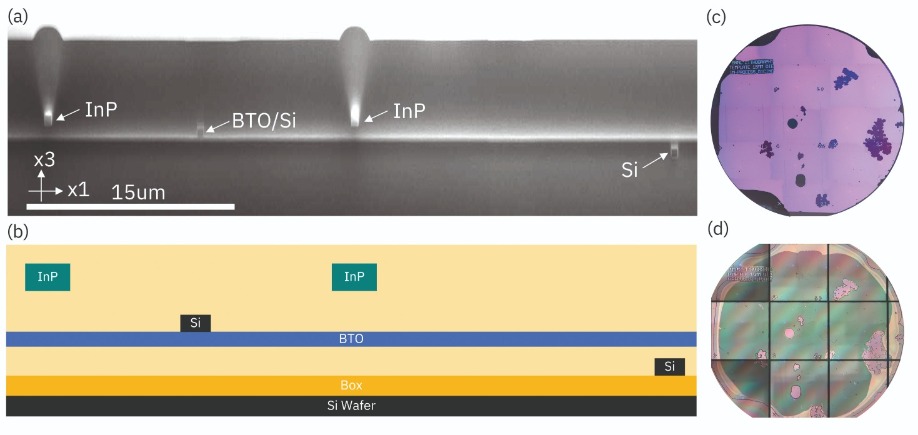
Figure 7. (a) and (b) Co-integrated waveguides in silicon, BTO/silicon and InP. (c) Wafer bonding of BTO/silicon (pink) on the silicon photonics acceptor wafer. Some defects, seen as dark areas, appeared during wafer bonding. (d) Wafer bonding of an InP layer (green colour) on top of the BTO/silicon layer. Defects in the BTO/silicon layer are transferred to the InP layer.
One of the keys to increasing coupling is to optimise the length of the tapers. At first glance, a very long taper is ideal, providing a small mode transfer loss, due to slow mode conversion – in the best case this process can be virtually loss free. However, long tapers are not a panacea, because they lead to a larger propagation loss in the waveguides in the coupling region, and they occupy a larger chip area.The sweet spot is the use of tapers that are as short as possible, but long enough to ensure that mode conversion is almost loss free. In our experiments, we have found that the coupling loss decreases with increasing coupler length (see Figure 8 (b)). This implies that we are yet to reach a taper length where propagation length dominates over mode transfer loss.
Coupling loss can be reduced even further by optimising the shape of the tapers. We have investigated this through simulation, considering optical modes in many equally distributed cross sections along the coupler structure (see Figure 9 (a)). Our studies consider the mode overlap between consecutive sections. When the mode overlap is large, the mode does not change much. However, when the overlap is small, there is a significant change in the mode field profile.
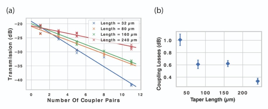
Figure 8. (a) Transmission as a function of the number of coupler pairs for different taper lengths for couplers between BTO/silicon and InP. (b) Coupling loss for BTO/silicon and InP couplers as a function of taper length
Based on these insights, mode transfer loss may be minimised by ensuring that the sections with a small mode overlap are longer, so that the mode field profile changes its shape slowly over the section length. On the other hand, sections with a large mode overlap can be shortened, helping to trim propagation loss.Drawing on mode overlap calculations, we have designed a taper containing three linear sections with different taper slopes. Using Lumerical Mode simulation software, we have found that the mode transfer efficiency exceeds 99.5 percent for 90 μm-long optimised tapers. Switch to a linear taper, and a length of 500 μm is required to deliver a similar performance. Or, to put in another way, by adopting an optimized shape we can slash the length of our taper by a factor of six while maintaining the mode transfer efficiency.
Targeting applications
Data centres and long-haul communication systems are generating strong demand for fast optical transceivers that are power- and cost-efficient. Using our platform, we can form high-performance transceivers from efficient transmitters and receivers.
Efficient transceivers are formed by generating continuous-wave optical signals with a III-V laser, subsequent modulation with a BTO/silicon electro-optical device, and turning to a silicon photonics platform to efficiently route, filter and multiplex the signals. If available, we can deploy electronic circuits for the integration of drivers for the laser and modulator. On the receiver side, we use a germanium-silicon photodetector – or, if we require a higher bandwidth, variants made with III-Vs. Here, the roles for silicon photonics circuits could include providing optical filters and demultiplexing circuits. In EPIC platforms, amplifiers and analogue-to-digital converter circuits might also be integrated.
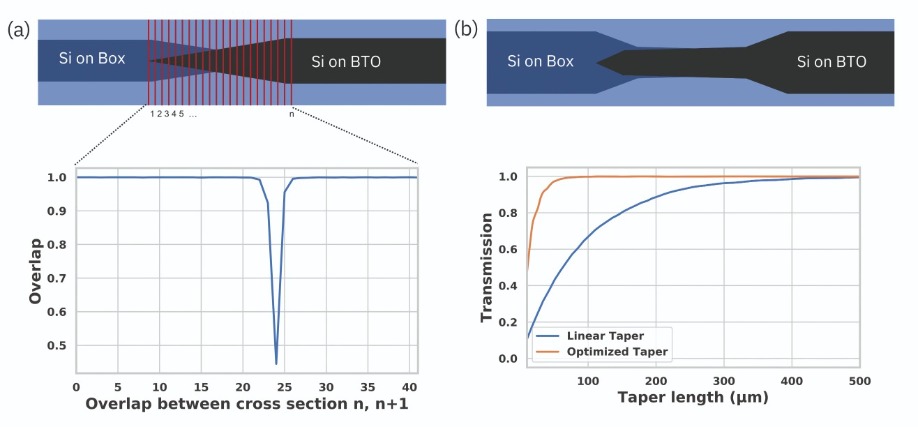
Figure 9.(a) Simulations of optical modes in 42 cross sections (red lines) along the taper. Mode overlap between consecutive sections were computed. (b) Simulated transmission for light coupling from silicon to a BTO/silicon layer as a function of taper length. A transmission value of 1 means that the mode is transferred without any loss. Using the optimised taper shape, a transmission exceeding 99.5 percent is realized for 90 μm-long tapers.
It is clear to see that armed with a platform featuring multiple functional layers, it is possible to combine the strengths of the existing silicon photonic ecosystem with novel functionalities for modulation, emission, and detection. This expansion in functionality also opens the door to radically new fields of applications, such as optical neuromorphic computing. We have started to consider this opportunity, exploring integrated, all-optical reservoir computing systems based on our co-integration platform (Figure 10). These reservoir computing systems are a special type of neural network, in which only the synaptic weights at the output layer are trained, while weights within the network are random but fixed.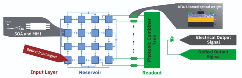
Figure 10. Concept for an all-optical reservoir computing system. Silicon photonics is used to route and mix signals between different nodes (blue squares). Semiconductor optical amplifiers (SOA) based on III-V technology provide a non-linear response at each node. Barium-titanate-based optical weights at the output of the reservoir tune signals, before they are united through a photonic combiner tree. The output signal is converted to the electrical domain using a III-V based photodetector.
Realising such networks requires the building of various blocks that are not available in standard silicon photonics. They include ultra-compact optical non-linearity or non-volatile optical weights. The good news is that semiconductor optical amplifiers based on III-V technology provide the required non-linear optical response, while BTO/silicon switches, which store their state in the ferroelectric domain configuration of the BTO film, can be used to form non-volatile optical weights. Applying large electric pulses tunes the domain configuration, which is retained for up to several days after the state is set. Uses of optical reservoir computing systems include compensating fibre-optic dispersion and performing Boolean operations, prior to the conversion of optical signals into the electronic domain by a transceiver.Our efforts have shown that by co-integrating BTO/silicon and III-V technology with silicon photonics we have created a very versatile photonic platform with novel optical building blocks. Results on this platform, featuring low-loss interlayer coupling, demonstrate for the first time the combination of three complementary but powerful technology platforms in a scalable, efficient manner. This multi-functional photonic platform enables not only efficient optical transceivers, but further exciting new applications, such as optical computing and signal processing.
We would like to thank Daniele Caimi, Felix Eltes, Yannick Baumgartner, Youri Popoff and Norbert Meier for their support for the fabrication of the coupling demonstrator. This project has received funding from the EU-H2020 research and innovation program under grants no. 688003 (DIMENSION), 688579 (PHRESCO) and 780997 (plaCMOS).
P. Stark et al. Heterogeneous Co-Integration of BTO/Si and III-V technology on a Silicon Photonics Platform. Optical Fiber Communication Conference (OFC) 2020, T3B.3. https://doi.org/10.1364/OFC.2020.T3B.3
S. Abel et al. Large Pockels effect in micro- and nanostructured barium titanate integrated on silicon Nat. Mater. 18 42 (2019) https://doi.org/10.1038/s41563-018-0208-0
F. Eltes et al. An integrated optical modulator operating at cryogenic temperatures. Nat. Mater. 19 1164 (2020) https://doi.org/10.1038/s41563-020-0725-5
Y. Baumgartner et al. Novel CMOS-Compatible Ultralow Capacitance Hybrid III-V/Si Photodetectors Tested up to 32 Gbps NRZ. Optical Fiber Communication Conference (OFC) 2019, Th3B.3. https://doi.org/10.1364/OFC.2019.Th3B.3
G. Van Der Sande et al. Advances in photonic reservoir computing. Nanophotonics 6 561 (2017) https://doi.org/10.1515/nanoph-2016-0132


