
Flying high with CPV
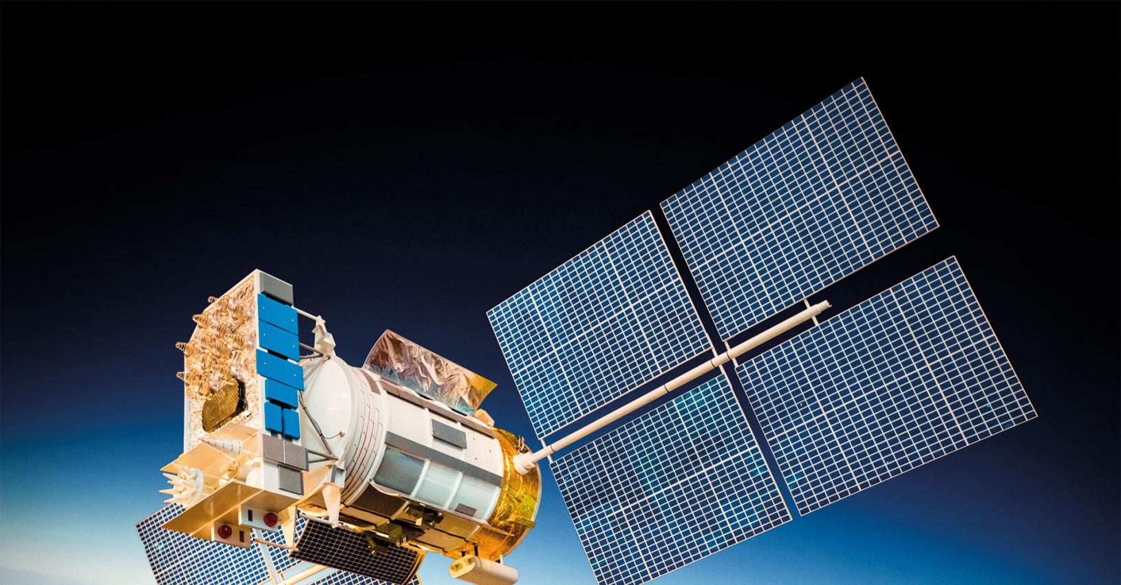
Operating at almost 100 suns, vast arrays of five-junction micro-concentrator cells promise to set a new benchmark for extra-terrestrial power
BY MATHEW LUMB FROM THE GEORGE WASHINGTON UNIVERSITY
While concentrator photovoltaics (CPV) is better known for its potential to deliver outstanding levels of power in sunny climes, it also has a number of compelling performance attributes for generating energy in space. Operating in the range of just ten to a hundred suns, CPV installed on-board a satellite or a space station has the potential to combine a remarkably high specific power, judged in terms of the Watts per kilogram, with a low cost-per-Watt and a high volumetric power density – that is, many Watts per cubic metre.
Thanks to these attractive assets, this form of power generation promises to offset the high launch costs for space deployment. It is well suited to this environment, because the use of a low level of concentration helps to maintain manageable cell operating temperatures and wide optical acceptance angles. And by incorporating focusing optics, there is a tremendous reduction in the impact of one of the harshest environmental aspects of space – particle irradiation. In a concentrator array, lenses made from radiation-hardened glass dramatically slow the degradation of photovoltaics by shielding the epitaxial layers from damaging radiation.
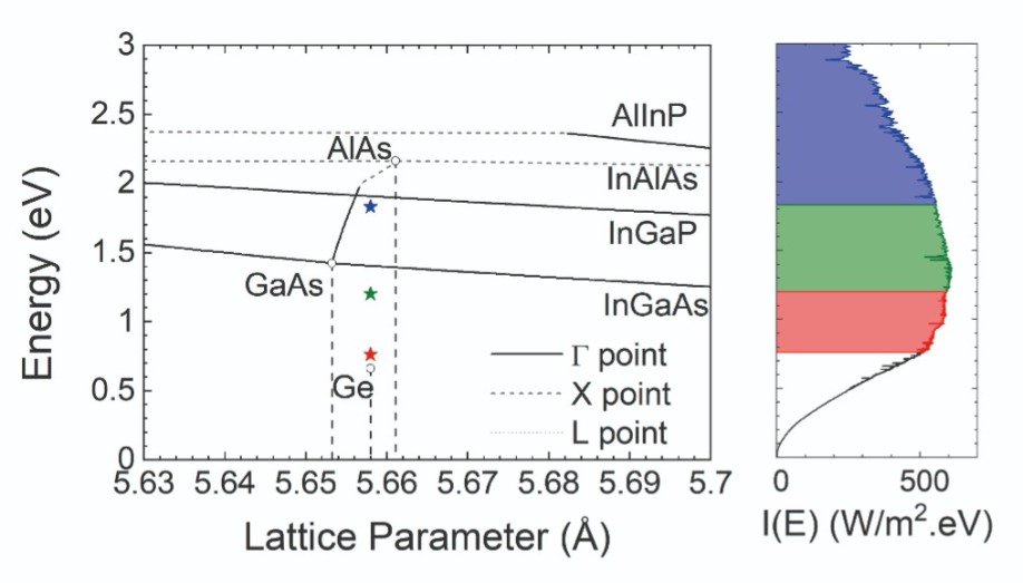
Figure 1. The ideal bandgaps for conversion of AM0 illumination from the detailed balance limit in a triple-junction solar cell, compared with available bandgaps of III-As and III-P alloys on germanium.
A particularly promising form of CPV uses solar cells with dimensions typically just 100-800 μm per side. When well designed, these microcells spread current efficiently across the cell aperture, eliminating the need for metal grid fingers. Another merit of these microcells is that they simplify thermal management, because their diminished dimensions enable effective heat dissipation along interconnect traces and into the backplane, lowering the temperature of these devices and increasing their efficiency. Microcells also permit miniaturised optics, which can be very lightweight and low in profile. Finally, the cells can be spaced close together to realise a micro-concentrator with a very high areal packing fraction and essentially no unusable area. Lengthening cell spacing also reduces the risk of arcing between adjacent cells, while providing a very high degree of flexibility in wiring configurations, which accommodates a large range of output voltages and currents while providing high tolerance to defects.Building on terrestrial success
Holding the record for the highest efficiency of all photovoltaic technologies are terrestrial concentrator systems. These are usually built around extremely high-performance, monolithic multi-junction solar cells. In these devices the solar spectrum is divided between the sub-cells, ideally in a manner that ensures a similar photocurrent from each, because this maximises efficiency.
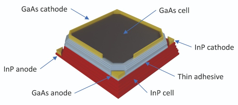
Figure 2. A stacked micro CPV cell, formed from separate GaAs and InP-based multi-junction solar cells, can form a four-terminal device.
For many years the workhorse of space photovoltaics has been a triple-junction cell based on the combination of InGaP, InGaAs and germanium. This architecture, closely related to a terrestrial CPV cell, is generally deployed without concentration thanks to the favourable economics of space power that are governed by high launch costs.On satellites, power tends to be produced by cells with a footprint of 25 cm2 to 80 cm2. Unfortunately, the suite of III-V alloys available on the lattice constant for germanium – the incumbent substrate for triple-junction space cells – fails to provide the ideal bandgaps for spectral splitting (see Figure 1). This has motivated researchers in academia and industry to develop alternative architectures that overcome these limitations. One material with much promise is the dilute nitride InGaAsN – it offers direct-bandgap alloys in the technologically important range of
1.4-0.8 eV that can be lattice-matched to both GaAs and germanium. Strain-balanced quantum wells also offer similar tunability, albeit over a smaller range.
Yet another option is metamorphic epitaxy, which underpins the record-breaking six-junction devices recently developed by scientists at NREL. However, with this class of device, it is very challenging to maintain high crystal quality and a good manufacturing yield.
-&-(d)-7ko880.jpg)
Figure 3. The mask layout for (a) the GaAs double-junction cell and (b) the InP triple-junction cell. (c) A microscope image of a printed five-junction solar cell using visible illumination and (d) the same cell viewed using near-IR illumination and an InGaAs camera. The GaAs materials are transparent in this image, revealing a uniform, void-free interface between the cells.
Today, there are a handful of commercial suppliers of III-V multi-junction solar cells. State of the art efficiencies range from roughly 29 percent for a basic germanium-based triple-junction space cell to around 32 percent for leading metamorphic devices. These efficiencies are for the solar spectrum received outside the Earth’s atmosphere, a condition known as air-mass zero, or AM0.Some of the highest-ever recorded efficiencies for multi-junction solar cells have involved the integration of materials grown on different substrates, such as GaAs, InP and GaSb. Adopting this approach allows III-Vs, which are lattice-matched to their native substrates using close to ideal bandgaps, to be fused into single devices.
Different materials can be united with wafer-bonded approaches. In the devices that result, current conducts across the heterointerface, with each subcell ideally generating a similar current. However, manufacturing devices with this approach is not easy, as high yield, low-resistance wafer bonding is notoriously tricky.
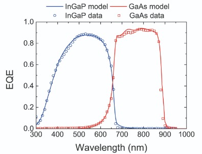
Figure 4. (a) Measured and simulated external quantum efficiency (EQE) for the GaAs double-junction cell. (b) Measured and simulated EQE spectra for the InP triple-junction cell. The implied EQE after stacking is shown by the dotted lines.
An interesting alternative is the heterogeneous integration of electrically isolated devices to form a four-terminal structure. This approach offers much freedom, as current-matching constraints are restricted to only subcells within the separate devices. Eliminating the requirement for electrical conductivity across the heterointerface therefore creates more flexibility in material choices.Printing cells
Another method for realising heterogeneous integration with a variety of micro-CPV cell material combinations is the highly parallel assembly technique known as micro-transfer printing. This approach for heterogeneous integration, pioneered by researchers at the University of Illinois at Urbana Champaign, has been advanced by our team, which is a collaboration between researchers at George Washington University, NRL, Semprius, X-Celeprint, Veeco, Northwestern, the University of Illinois at Urbana-Champaign and MIT.
Our capabilities, refined over several years, include the development of a micro-transfer printing process for placing fully-functional, GaAs-based PV dice (known as chiplets) on top of InP or GaSb-based cousins to make a four-terminal device (see Figure 2).
The printing process begins by using a selective chemical etch to release chiplets from their native substrate, whilst they are temporarily tethered in place with a photoresist. An elastomer stamp picks up the chiplets before adhering them to a non-native substrate, in this case another micro-CPV device. An extremely thin polymer adhesive, less than 20 nm-thick, forms a permanent bond.
We use a tool developed by X-Celeprint to carry out the fully automated printing process. This partner has commercialised transfer printing technology, drawing on experience from a long-time collaboration with former micro-CPV company Semprius. One of the primary merits of the printing process is that it liberates PV devices from their expensive growth substrates, which can be reused.
Our latest solar cells, incorporating both GaAs-based and InP-based devices, were designed using an analytical drift-diffusion model incorporating photon recycling and coherent optical effects. Using a commercial Veeco K475i MOCVD tool we fabricated both devices, presenting results at this year’s SPIE Photonics West conference in San Francisco.
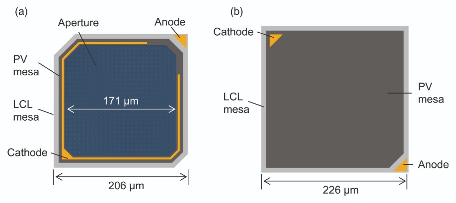
The GaAs part of the cell consists of a pair of junctions, made from InGaP and GaAs, separated by an AlGaAs/GaAs tunnel junction. At the bottom of the device we include an AlInP epitaxial release layer. Using a highly selective etch, we remove this layer and release die from their native substrates prior to transfer printing. We produce square-shaped solar cells with sides of around 200 μm, using dry etching in an inductively coupled plasma tool to define mesa dimensions. The front metal pattern forms a roughly square aperture with a width of 171 μm (see Figure 3 (a) and (b)). We improve the efficiency of the cell by applying a three-layer SiO2/Si3N4/TiO2 anti-reflection coating, and we increase the device’s robustness by passivation. This involves depositing Si3N4/SiO2 over the sidewalls.
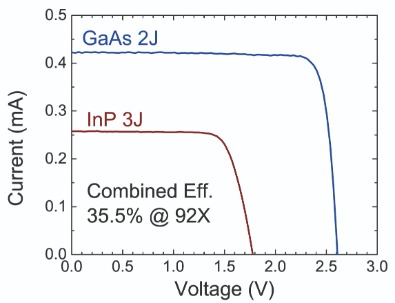
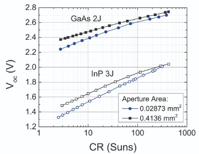
Figure 5. (a) Light current-voltage (I-V) curves for the stacked GaAs- and InP-based multi-junctions, which give a combined efficiency of 35.5 percent under simulated AM0 illumination. (b) Measured open-circuit voltage (Voc) for microcells with different perimeter-to-area ratios, highlighting the losses at low concentration due to perimeter recombination.
The InP part of the cell is formed from three n-on-p junctions. The top two junctions consist of lattice-matched layers of InGaAsP, with bandgaps of 1.18 eV and 0.97 eV. The bottom junction is made from InGaAs with a band gap of 0.74 eV. Separating the junctions are p++ InGaAs/n++ InP tunnel junctions. Dissimilar to the GaAs cells, the InP triple-junction cell does not contain a sacrificial layer for epitaxial lift-off. Due to this, all our measurements are performed on native InP substrates. Note that highly selective etch combinations do exist in the InP family, so there is no barrier to producing printable InP-based triple-junction cells using the same process employed for making the GaAs cell.Scrutinising our fabrication process using visible and near infrared microscopy reveals precise alignment with a void-free interface between the cells (see Figure 3(c) and (d)). Measurements of the external quantum efficiency curve for our devices, using larger area cells from the same wafer, are in good agreement with our simulations (see Figure 4).
Obtaining a reliable figure for the external quantum efficiency of the stacked cells is difficult, due to significant leakage produced by the microcells at the very low light levels employed for this measurement. Our workaround is to deduce the external quantum efficiency of our stacked devices by correcting the experimental data for the transmission through the GaAs heterostructure. While this is not a direct measurement of the external quantum efficiency, it can accurately reproduce the measured light-current-voltage characteristics for stacked and unstacked devices. As expected, the external quantum efficiency of our InP-based cell increases after stacking, because it benefits from the antireflection coating on the GaAs cell. The light that reaches the underlying InP cell has been filtered by absorption in the GaAs layers, which have a cut-off at roughly 870 nm.
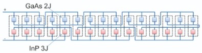
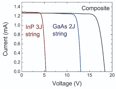
Figure 6. (a) A possible interconnection layout to produce a current-matched, two-terminal layout using 15 CPV cells. (b) The predicted composite current-voltage (I-V) curve, neglecting cell-to-cell variation.
We have measured the photocurrents of all five subcells. Values for InGaP and GaAs in the GaAs-based devices are 16.9 mA/cm2 and 15.8 mA/cm2, while the top, middle and bottom cells for the InP-based device recorded current densities of 9.5 mA/cm2, 9.9 mA/cm2 and 12.5 mA/cm2, respectively.To characterise the light, current and voltage performance of our cells, we have used a collimated AM0 solar simulator with a plano-convex lens to focus the light. We determined the incident intensity of the simulated solar spectrum using the ratio of the measured short-circuit current to the equivalent value for 1 sun, as determined from external quantum efficiency curves combined with the AM0 spectrum. This methodology revealed a peak four-terminal efficiency of 35.5 percent at 92 suns.
Greater insight into the performance of our five-junction cell is provided by the current-voltage characteristics of separate InP and GaAs cells operating at 92 suns under AM0 illumination (see Figure 5(a)). Based on these results, our modelling suggests realistic efficiencies in excess of 38 percent at concentrations below 100 suns are within our grasp if we improve current balancing of our subcells, increase the transparency of the tunnel junctions and optimise the material quality of the InGaAsP alloys. When combined with lightweight CPV optics, this high conversion efficiency has the potential to enable extremely high specific-power space arrays which, when combined with the advantages in radiation resistance, areal fill factor, low arcing risk, low cost and high volumetric power density, will provide strong competition to incumbent technologies based on conventional, large-area solar cells.
We are working hard to continue to improve our devices. Current efforts include: developing highly doped C:InAlAs for use in the InP-based tunnel junction, which will improve optical transmission and lower series resistance in the InP triple-junction cell; and tuning subcell thicknesses to optimise the current balancing between the subcells.
A drawback of microcells is their high perimeter-to-area ratio, which creates excessive leakage current at low light intensities. At a very high sun concentration this is not an issue, with leakage effects suppressed by a favourable light-current to dark-current ratio. But in the relatively low concentration regime, desirable for the space micro-concentrators that we are pioneering, we need to consider perimeter recombination.
To evaluate the extent of this issue, we have compared open-circuit voltages of devices with sides of 200 mm and 700 mm. These measurements, conducted at a range of concentrations, show that there is a reduction in open-circuit voltage in the smaller devices, due to the increased dark current – and this shortfall in performance is exacerbated as the concentration decreases.
It is worth noting that our GaAs devices have a Si3N4 dielectric covering their sidewalls, which provides passivating properties, while the InP device sidewalls are bare. This lack of dielectric is behind a drop in open-circuit voltage of 3 percent for the InP-based cells operating at 100 suns, compared with just 1.6 percent for the GaAs-based devices. There is no doubt that trimming sidewall leakage will yield performance improvements in our microcells with sides of around 170 μm. One important goal for us is to address this by developing strategies to minimise perimeter recombination.
Whilst four-terminal stacked cells provide simplifications in assembly, they are not ideal in most practical PV array scenarios. That’s because operating two separate strings of multi-junction solar cells at their respective maximum power points is impractical, due to the additional complexity and hardware required. Our solution is to combine separate devices into a small-integer series or parallel string combinations which, when combined, match the photocurrents of the GaAs and InP cell strings. This results is an efficient, two-terminal output.
We are able to implement this approach by drawing on the interconnection degrees of freedom afforded by the micro-CPV architecture. Consider, for example, an array of our 170 μm CPV cells with a geometric concentration ratio of 92. This has a density of almost 380,000 cell-and-lens units per square metre, providing tremendous flexibility in wiring options.
To realise a roughly current-matched string for our five-junction cell we connect five series-connected groups of three GaAs double-junction cells, arranged in parallel, to three series-connected groups of five InP triple-junctions, configured in parallel. We calculate that the 15 stacked cells arranged in this manner will deliver more than a milliamp, with an associated output voltage of more than 15 V (see Figure 6 (a) for a diagram of the stacked cell arrangement, and Figure 6 (b) for the calculated light, current and voltage characteristics, using measured current-voltage curves at 92 suns).
By combining groups of this 15-cell unit in series or parallel as part of a larger array, we can provide flexibility in output voltage and current whilst retaining two terminals. There is also the option to use different photocurrent ratios by adapting cell design; for instance, in previous work we explored a terrestrial design for a stacked five-junction solar cell with a ratio of photocurrents between the GaAs and the InP cells of 2:1. Our work showcases some of the compelling advantages of micro-CPV over incumbent space photovoltaic technologies. By employing micro-transfer printing for assembly, we have a well-considered manufacturable route to high-efficiency heterogeneously integrated CPV cells. Our latest results demonstrate a conversion efficiency of
35.5 percent under concentrated AM0 illumination, and we have set out a clear pathway to efficiencies
in excess of 38 percent. Realising this with lightweight, low-profile optics gives us the opportunity to break new ground in the key metrics of specific power, end-of-life efficiency and cost. We are well on our way to disrupting the
long-established technological approaches for space power.
The information, data, or work presented herein was funded in part by the Advanced Research Projects Agency-Energy (ARPA-E), US Department of Energy, under Award Number DE-AR0000882. Research performed in part at the NIST Center for Nanoscale Science and Technology NanoFab.
M.P. Lumb, Sending CPV into Space, Compound Semiconductor Magazine, Nov&Dec 2018, 36-40.
X. Sheng et al. Nature Materials 13 593 (2014)
M. Steiner et al. IEEE Journal of Photovoltaics 6 1020 (2016)
J.F. Geisz et al. Nature Energy 5 326 (2020)
M.P. Lumb et al. Towards the Ultimate Multi-Junction Solar Cell Using Transfer Printing, in: 43rd IEEE Photovoltaics Specialists Conference, IEEE, Portland, OR, USA, 2016, pp. 40-45
M.P. Lumb et al. Advanced Energy Materials 7 1700345 (2017)
M.P. Lumb et al. J. Appl. Phys. 116 194504 (2014)
M.P. Lumb et al. Design, modeling, and experimental results for CPV arrays built using heterogeneously integrated III-V micro-cells, Proceedings 11275 Physics, Simulation, and Photonic Engineering of Photovoltaic Devices IX; 1127504 (2020)
J.E. Moore et al. J. Photon Energy 9 014501 (2019)


