
Evaluating new switching technologies

It takes more than a change in part number to move to a wide bandgap technology; what’s required is a systemic approach, considering all aspects of design
BY STEFAN OBERSRIEBNIG FROM INFINEON TECHNOLOGIES
TRANSISTORS ARE EVERYWHERE. They are in our mobiles, tablets and PCs, providing the key ingredient in integrated circuits, with each device tuned for a specific function, such as fast switching or a low operating voltage. Transistors also appear in a discrete form, serving in power switching applications. Here there is also a need for optimisation, a task made more challenging by an ever-growing range of products. But select the right one and the rewards are greater than ever.
This expansion in the range of power transistors has taken place against a backdrop of ‘More than Moore’, an era where the use of new materials offers a route to improved performance. During this time, we have learnt that the latest fabrication node may not provide the most optimal solution; instead, it may be more prudent to choose the appropriate node for each function and integrate at a modular level.
When it comes to discrete transistor technologies, particularly for high-power applications, the expansion in choice comes from the introduction of new materials. It may be perceived that the technologies on offer, namely silicon, SiC and GaN, follow a path comparable to integrated digital transistors; that each new step is a linear improvement on the last, and should be adopted without question as the right replacement. But this is a misconception. The reality is more nuanced, with the optimal solution hinging on adopting the lessons learned through the development of More than Moore to the power domain. One must not simply view the newest technology as the best, without first giving it closer inspection. When engineers do this, they need to consider many aspects associated with design, so that they select the technology that is best for the respective application.
For makers of silicon, SiC and GaN power electronic devices, two of the biggest applications are power conversion and power management. Many devices are deployed in conversion topologies, based on variations of the common switched-mode power supply. The basic switched-mode power supply takes advantage of a transistor’s ability to turn on and off rapidly and precisely, with variants manipulating specific features to deliver higher efficiency under specific conditions. New wide bandgap technologies are enabling innovative ways to exploit these topologies through faster switching and higher power capabilities.
It is often overlooked that even without changes to switching frequencies and turn-off/turn-on timings, the replacement of silicon devices with those with a wider bandgap can still deliver improvements. These gains relate to specific features, such as the integrated body diodes of SiC MOSFETs that allow them to take the place of conventional diodes in synchronous rectification designs. Merits of the body diode of the SiC MOSFET include a negligible reverse recovery charge and a high forward-voltage drop when conducting, which dissipates the energy build-up that limits the switching frequency of silicon devices. It is the switching characteristics of SiC that are behind its capability to deliver higher efficiency.
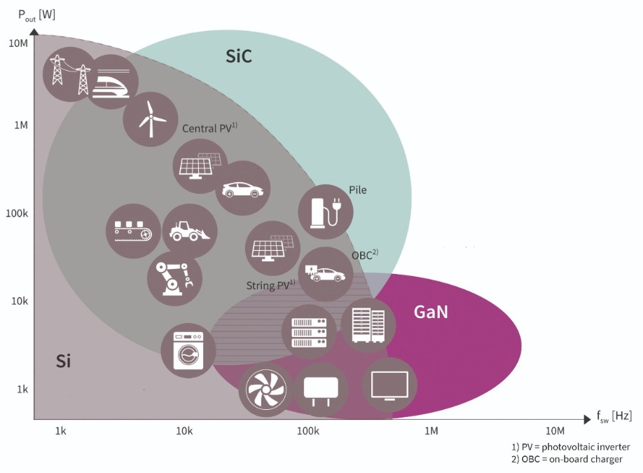
Figure 1: Mainstream silicon, complemented by SiC and GaN, delivers increased efficiency and a higher power density.
Many different types of switching topology are in use today, including inverters, active clamp flyback converters and phase-shifted bridge topologies. This diversity is unlikely to change, as each topology has its own merits.
When designers select a topology, their decision tends to be governed by the requirements of the application rather than the ideal substrate. Due to this hierarchy within the decision-making process, GaN is not always the best option for applications requiring high voltages and currents. The reasoning is that although GaN is better than silicon in half-bridge topologies when implementing hard-switching, SiC has the upper hand for soft- and resonant-switching topologies (see Figure 1 for an evaluation of the suitability of today’s available semiconductor technologies to several key applications).
As new applications emerge, such as electric vehicles and renewable energy, and existing applications evolve, like data centres and cellular telecommunications, the requirement isn’t simply for more power. Instead, there is a need for more power, delivered in the same or a smaller form factor, using different voltage levels, currents, stability and response times. This list of requirements puts pressure on power supply developers, who may need to explore new topologies. However, the demands also create an opportunity to evaluate new transistor technologies for fulfilling these needs.
Figure 2: Different power switching technologies and application areas.
At a high level there is much to be garnered by considering the characteristics of all the classes of transistor technology. Taking this approach provides a snapshot of their respective merits and goes some way to explaining why the industry is pursuing their development.Transistor characteristics
At Infineon Technologies, a multi-national device manufacturer operating in the power electronic industry, we have devoted much time and effort to developing a range of technologies based on silicon, SiC and GaN, as well as the corresponding drivers needed to maximize the potential of each technology. We have a rich history of innovation, including invention of Superjunction technology and the launch of the world’s first SiC Schottky barrier diode (in Figure 2 we offer a graphical representation of where each semiconductor technology fits in terms of power transistors).
Our experience is that the demand for silicon-based power devices remains strong. It is still the best technology for many applications, and it has reached a level of maturity that makes it highly cost-competitive. Although at one stage regular silicon appeared to be running out of steam, the introduction of superjunction technology injected a new lease of life, reducing the on-resistance. This led to a trimming of switching losses, allowing this class of device to serve in high-voltage, high-power applications.
When SiC launched, it lowered the on-resistance of the transistor for a given area by a factor of three. Another advantage, also coming from its wider bandgap, is that it enabled devices to handle far higher voltages without failure.
Recently, GaN has entered the fray, sporting a very similar bandgap to SiC. However, its transistor architecture is markedly different from that of SiC MOSFETs and superjunction devices. GaN FETs feature an undoped layer that increases electron mobility and results in an even lower on-resistance.

At first glance, the reductions in on-resistance associated with moving from silicon to SiC and then on to GaN suggest that the latter is always the preferred solution for power switching. However, while the material used for the transistor determines its strengths, the characteristics of each class of device differ under the same operating conditions. Due to this, when GaN is employed in a topology implementing a continuous conduction mode, it only delivers a superior efficiency to a silicon MOSFET under certain load conditions. So, when designers make a decision, they must take into account how the technology behaves under all operating conditions; they should not view any two technologies as drop-in replacements for one another.
With these factors at play, designers must evaluate the difference in the performance of SiC, of GaN and of silicon MOSFETs and superjunction devices in different types of power-converter circuits – the right approach for one application is not necessarily the right one for another. Due to this, the best results do not come from simply standardizing on one wide bandgap technology, as this will not lead to efficiency gains across all applications.
We are in an enviable position of offering industry-leading devices made from silicon, SiC and GaN; and we can draw on our system expertise to support our customers through every generation of their application. This allows us to supply the best technology for the most appropriate topology, whether that is silicon, SiC or GaN, making us a great power-design partner. We can advise what will provide the best cost-to-performance ratio – it may be silicon; in some high-power applications it could be SiC; and in other scenarios – for instance for high frequency designs, GaN might deliver the best performance, making it the right option.
Note that the right decision is not set in stone. SiC and GaN are still evolving, and it is also crucial to consider the driver technology used for power switching, as matching the best transistors with the best drivers plays a big part in optimising design.
Power integration
Each application comes with its own requirements, which dictate the right topology and in turn the most appropriate semiconductor technology. However, there is also a trend towards more integrated solutions, which combine transistors and drivers into modular solutions. In much the same way as More than Moore is bringing together the most appropriate nodes for given functions, power modules are starting to simplify power supply design for various applications with similar requirements.
The semiconductor industry is moving towards greater integration at a modular level. This is already apparent in the wireless communication sector, where entire radio systems are being integrated closely alongside controllers, allowing the end device to pass certification with less effort. In many cases, wireless modules are supplied pre-certified, making them a ‘plug and play’ solution.
Within the power systems sector, a similar trend is underway and set to continue. We are well-positioned to respond, thanks to a portfolio of products and the experience required to develop and bring to market high-quality integrated power modules.
Merits of power modules are not limited to simplifying the design process for the customer. By optimising the design, we also provide two major performance benefits: a reduction in size compared with discrete components, resulting in higher power density at ‘no extra cost’; and a higher efficiency, which is an overriding requirement in power conversion and one of the key drivers behind the development of wide bandgap technology.
Using a module also has practical benefits. It is not easy for an engineering team to realise a high level of efficiency, because they need to understand how the power supply will behave under all possible modes of operation when selecting the design that delivers a performance curve that best fits their objectives. With discrete devices this could be an iterative process, with no guarantee that the results deliver the best efficiency under all operating conditions. By turning instead to a power module, complexity is eliminated, allowing an out-of-the-box solution to deliver a superior efficiency while increasing ease of use.
There is no doubt that the introduction of wide bandgap semiconductor technologies improves the power conversion landscape. They are complementing silicon-based technology by extending power and switching frequencies to
support new applications with improved topologies. However, they must not be seen as a drop-in replacement for existing technologies. It is also critical that the underlying requirements of the application define the switching topology used and in turn guide engineers in their selection of the best transistor technology for meeting power efficiency goals.
We have an incredibly strong track record in the power semiconductor industry, having more than 40 years of power MOSFET know-how at our hand. Our portfolio includes silicon, SiC and GaN power devices, plus optimised complementary drivers. We continue to expand our offering, with recent steps in this direction including the acquisition of Cypress Semiconductor, which will increase our offering at the system level. By putting all of this experience into practice, we are uniquely positioned as a trusted advisor and partner within the semiconductor industry.


