
Taiwanese firm orders second ClassOne System
Solstice electroplating system will be used to produce Heterojunction Bipolar Transistors and VCSELs
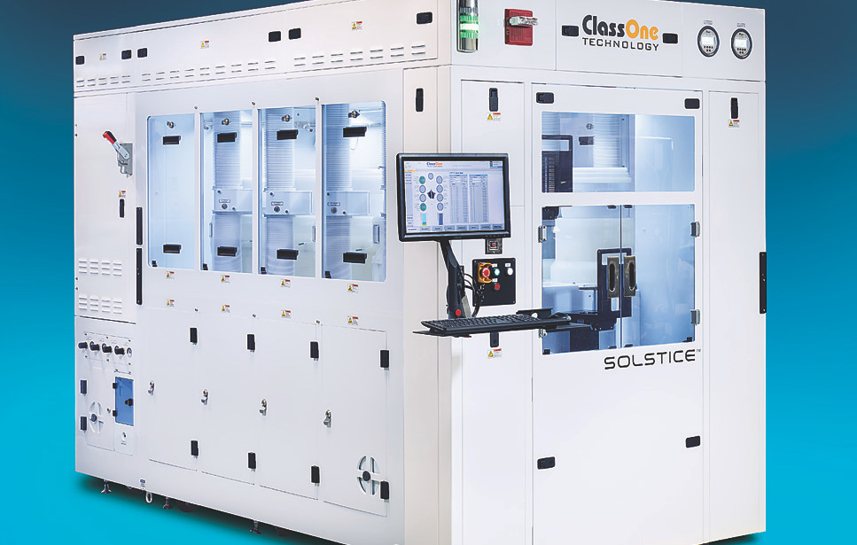
Semiconductor equipment manufacturer ClassOne Technology announced the sale of its Solstice S8 electroplating system to a major semiconductor foundry service based in Taiwan. This is the second S8 to be purchased by the company. The 8-chambered Solstice platform is designed specifically for ≤200mm wafer processing. The new tool will be used to produce Heterojunction Bipolar Transistors (HBTs) and VCSELs. The announcement was made by ClassOne’s CEO, Byron Exarcos, and senior technology director, John Ghekiere.
“This user is a high-volume semiconductor manufacturer,” said Ghekiere. "So they are interested not only in the Solstice's superior plating performance, but also in its reliable, fully-automated high throughput. The tool is being used for wafer level packaging processes, including copper pillar and solder bump electroplating.”
“This customer has been using our Solstice S8 electroplating equipment for several years now," said Exarcos. “The tool has been fully qualified for their processes and is meeting their aggressive performance goals. Now, their business is rapidly expanding, and they've chosen to bring in a second S8 to support that growth. We're actually seeing this pattern across the industry today. As Solstice is becoming embedded into customer processes, the repeat orders are coming in with increased frequency. We're very gratified by this vote of confidence in the Solstice and in ClassOne.”
Ghekiere noted that today’s HBT devices are used in many ultrafast circuits and those requiring high power efficiency, including next-generation RF power amplifiers, 5G cellular phones, etc. VCSELs are used in 2D and 3D imaging, facial recognition, smart-glasses, fibre optic communications, LiDAR, and much more.
The ClassOne Solstice S8 is an 8-chamber system for high-performance, fully-automated electroplating and surface preparation. The Solstice series, which was specifically designed for ≤200mm wafer processing, also includes the S4, which provides up to four processing chambers, and the LT, with up to three chambers. In addition to electroplating, the tool’s special Plating-Plus capabilities enable it to handle a number of other surface preparation functions, including wafer cleaning, high-pressure metal lift-off, resist strip, UBM etch and more. This multi-processing flexibility serves to streamline process production and can reduce the number of different tools a user needs to purchase.


