
EC invests €20M in next generation electronics
Launches first experimental pilot line for graphene and 2D layered materials
The European Commission (EC) has announced a €20 million investment in the next generation of electronics and semiconductors. The 2D Experimental Pilot Line (2D-EPL) was announced officially on February 4, 2021, as the first graphene foundry to integrate graphene and layered materials into semiconductor platforms. The new project aims to keep Europe at the forefront of this technological revolution.
Born within the innovative ecosystem pioneered by EU-funded project, the Graphene Flagship, the 2D-EPL will cover the entire value chain, from tool producers and chemical and material providers to manufacturing lines. This collaborative project will integrate several Graphene Flagship members to pioneer the fabrication of new prototype electronics, photonic devices and sensors integrating graphene and layered materials.
The 2D-EPL will offer comprehensive prototyping services to companies, research centres and academics, so they can develop and test their innovative technologies based on 2D materials.
“By developing a European pilot line for the processing of graphene and layered materials, we aim to bring these innovative materials from the academic laboratories to the semiconductor production lines, making them compatible with the standards in the industry,” explained Cedric Huyghebaert, technical leader for the 2D-EPL project, and programme manager for exploratory material and module integration at imec, Belgium.
“Moreover, we want to offer early access to experimental pilot line production to the innovative graphene community in Europe. The pilot line will allow them to scale up the production of their innovative devices based on graphene and layered materials.”
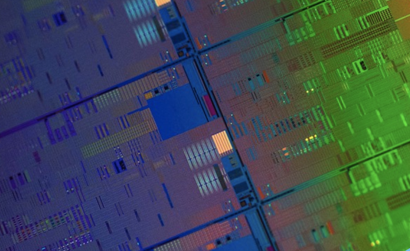
Combining graphene and 2D materials with silicon could enhance the potential of electronic technologies, traditionally based on silicon. Nevertheless, integrating both materials at a large scale has been challenging, and up to now advances have progressed at a slow pace, due mostly to a lack of infrastructure. The 2D-EPL will address this challenge, allowing manufacturers to control the interfaces between silicon semiconductors and 2D materials on a large scale.
The 2D-EPL will develop the tools, chemistry and materials required for the integration of graphene and layered materials on established semiconductor platforms, which use silicon technologies. The ecosystem and procedures will be validated in state-of-the-art cleanroom environments all around Europe, such as AMO and iHP, Germany; VTT, Finland; and imec, Belgium.
In a later phase, the project will also develop modules to manufacture the basic building blocks for graphene and layered material-based technologies in the fields of optoelectronics, photonics and electronics. These modules will be publicly available for European users through multi-purpose wafers. This strategy will guarantee that these novel technologies are widely available and accessible at a reasonable cost.
The ultimate goal of the 2D-EPL is to build demonstrators and achieve low volume production of innovative graphene and layered material-based technologies integrated with traditional semiconductors, working closely together with leading Graphene Flagship partners across Europe, including SMEs, industrial companies, research institutions and academic partners.
“For many applications, the wafer scale integration of graphene and potentially other 2D materials is required for products to appear on the market,” explained Lilei Ye, business developer for Electronics Applications at the Graphene Flagship. “The 2D-EPL will accelerate the manufacture of new prototypes for electronics, photonics and optoelectronics with integrated graphene and layered materials.”
”The 2D-EPL really highlights how the European Commission, through projects like the Graphene Flagship, can make an impact in European research, development and industry,” said Graphene Flagship Director Jari Kinaret. “We identified a challenge – upscaling the production of graphene electronics — and the European Commission heard us, finding funding to address this challenge.”
A large number of partners participating in the new adventure, the 2D-EPL, are also active members of the Graphene Flagship, one of the largest research initiatives ever funded by the European Commission.
The 2D-EPL will work closely with the Graphene Flagship to understand the fundamentals of graphene and layered materials and establish a plan to bring these materials to the market.


