
Scaling up large-area integration of 2D materials
European researchers report a new method to integrate graphene and 2D materials into semiconductor manufacturing lines
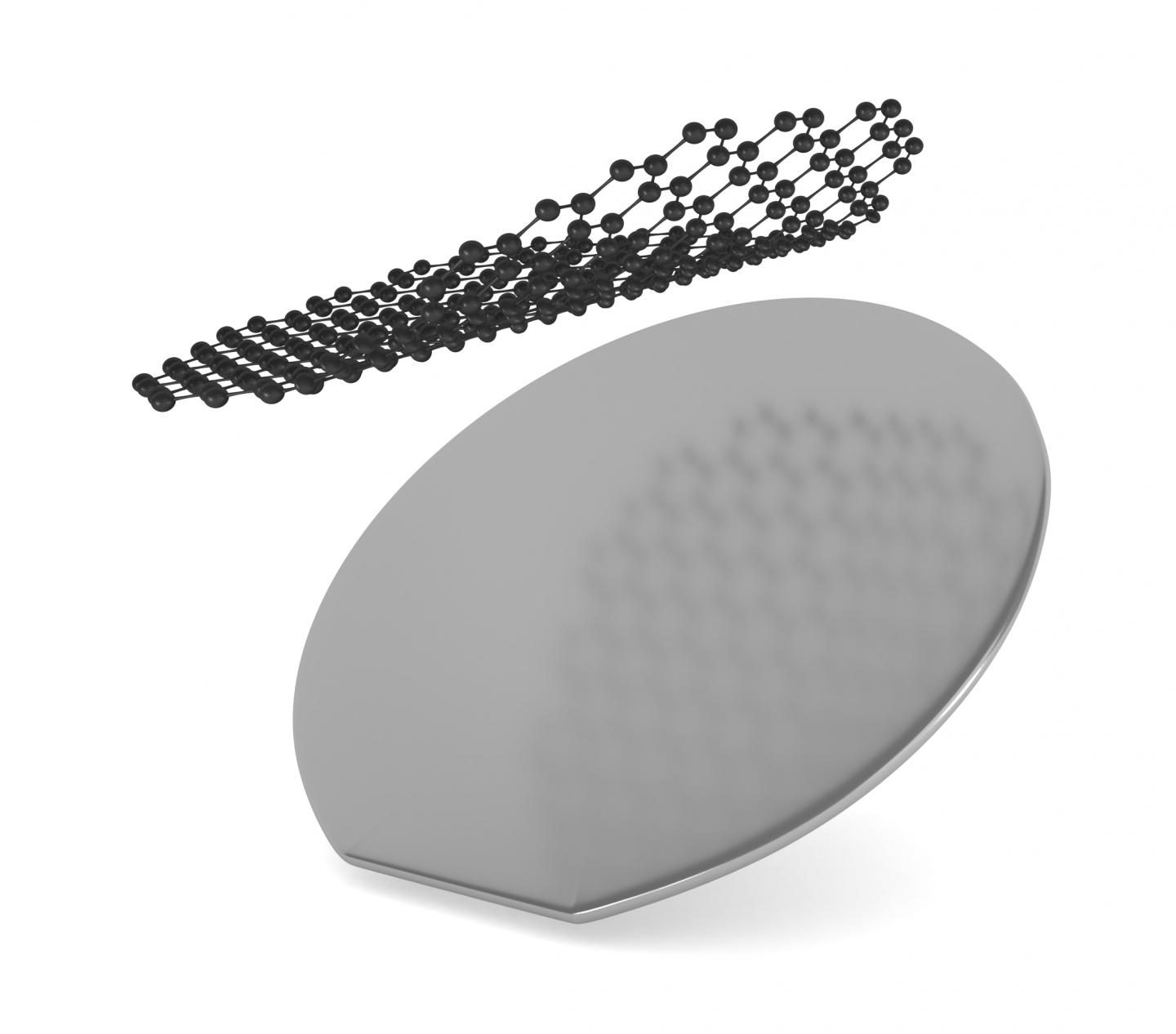
2D materials have a huge potential for providing devices with much smaller size and extended functionalities with respect to what can be achieved with today's silicon technologies. But to exploit this potential we must be able to integrate 2D materials into semiconductor manufacturing lines - a notoriously difficult step. A team of Graphene Flagship researchers in Sweden and Germany now reports a new method to make this work.
The technique, just published in Nature Communications by researchers from Graphene Flagship partners RWTH Aachen University, Universität der Bundeswehr München and AMO GmbH, in Germany, Graphene Flagship Associate Member KTH Royal Institute of Technology, in Sweden, in collaboration with Protemics GmbH.
The integration of 2D materials with silicon or with a substrate with integrated electronics presents a number of challenges. "There's always this critical step of transferring from a special growth substrate to the final substrate on which you build sensors or components," says Arne Quellmalz, researcher at Graphene Flagship Associate Member KTH and lead author of the paper. "You might want to combine a graphene photodetector for optical on-chip communication with silicon read-out electronics, but the growth temperatures of those materials is too high, so you cannot do this directly on the device substrate."
So far, most of the experimental methods for transferring 2D materials from their growth substrate to the desired electronics are either non compatible with high-volume manufacturing or lead to a significant degradation of the 2D material and of its electronic properties. The beauty of the solution proposed by Quellmalz and co-workers is that it lies in the existing toolkits of semiconductor manufacturing: to use a standard dielectric material called bisbenzocyclobutene (BCB), along with conventional wafer bonding equipment.
"We basically glue the two wafers together with a resin made of BCB," explains Quellmalz. "We heat the resin, until it becomes viscous, like honey, and press the 2D material against it." At room temperature, the resin becomes solid and forms a stable connection between the 2D material and the wafer, he says. "To stack materials, we repeat the steps of heating and pressing. The resin becomes viscous again and behaves like a cushion, or a waterbed, which supports the layer stack and adapts to the surface of the new 2D material."
The researchers demonstrated the transfer of graphene and MoS2, as a representative for transition metal dichalcogenides, and stacked graphene with hexagonal boron nitride (hBN) and MoS2 to heterostructures. All transferred layers and heterostructures were reportedly of high quality, that is, they featured uniform coverage over up to 100-millimetre sized silicon wafers and exhibited little strain in the transferred 2D materials.
"Our transfer method is in principle applicable to any 2D material, independent of the size and the type of growth substrate", says Max Lemme, from Graphene Flagship partners AMO GmbH and RWTH Aachen University. "And, since it relies only on tools and methods that are already common in the semiconductor industry, it could substantially accelerate the appearance on the market of a new generation of devices where 2D materials are integrated on top of conventional integrated circuits or microsystem. This work is an important step towards this goal and, although many further challenges remain, the range of potential applications is large: from photonics, to sensing, to neuromorphic computing. The integration of 2D materials could be a real game-changer for the European high-tech industry."
Recently, the European Commission launched a €20 million project to bridge the gap between lab-scale manufacturing and large volume production of electronic devices based on two-dimensional materials, the Graphene Flagship 2D Experimental Pilot Line (2D-EPL). "This paper is a good example of the work that we carry out in the 2D-EPL project," says Cedric Huyghebaert, program manager for exploratory materials and module integration at Imec and technical leader of the 2D-EPL project. "This is one of our urgent tasks at the moment is to develop tool kits and design manuals for manufacturing devices based on 2D materials that are compatible with the standards of semiconductor industry", says Huyghebaert. "The next step will be to demonstrate the potential of these processes for producing innovative sensors and optoelectronic devices on a pilot line."


