Loading...
News Article

Jeol enhances SEM Sample Preparation

News

New configuration of broad ion beam milling cross section polisher includes high-speed milling, sputter coating, cryo-preparation and air-isolated transfer

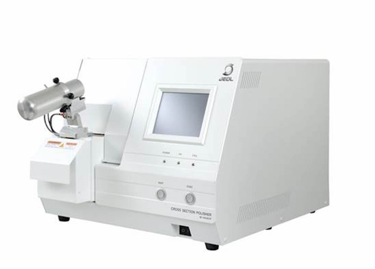
Jeol USA has introduced a new configuration of its broad ion beam milling instrument, the cross-section polisher (CP). The CP is widely used for preparing pristine samples prior to high resolution imaging and elemental analysis with the scanning electron microscope (SEM).

The upgraded configuration includes high-speed milling, sputter coating, cryo-preparation (down to LN2 temperature) and air-isolated transfer for atmosphere sensitive specimens (for example Li batteries).

Traditional mechanical preparation of specimen surfaces for SEM imaging can introduce various artifacts, such as scratches and embedded polishing media, that obscure the original microstructure, crystallographic information and precise layer thickness measurements. Broad ion beam polishing using the JEOL cross-section polisher (CP) offers pristine surface preparation with minimal artifacts.

The Jeol CP is a tabletop instrument suited for preparation of a variety of environment and beam sensitive materials, including metals, polymers, ceramics and composites.

The instrument offers the ability to mill large samples with wide area preparation (up to 8 mm wide cross-sections). It features the option to choose ion beam accelerating voltage of up to 10kV with up to 1.2 mm/hr milling rate. The system is easy to set up and can be programmed for high-speed processing and finishing of high-quality cross sections in a short period of time. Popular features such as intermittent milling (automated duty cycle for beam sensitive specimens) and fine milling (low voltage fine finish of specimen surfaces, ideally suited for techniques such as EBSD) are included in a standard configuration.

The CP polisher is equipped with a newly designed multi-purpose stage to fulfill increasingly diversified market needs and allow multi-functionality by utilizing a variety of specimen holders. Surface milling and polishing, cross-section polishing as well as carbon or metal sputter coating are now possible within one instrument, using specialized functional holders.

“Jeol has been a pioneer in the field of easy and accessible broad ion beam specimen preparation for SEM, with over 1900 units sold world wide,” says Natasha Erdman, SEM and Ion Beam product manager at Jeol USA. “We have been continuously improving the instrument to make it more versatile while providing a streamlined workflow for our customers. With inclusion of high-speed milling, cryo capabilities and air-isolated transfer Jeol is providing our customers with innovative tools to meet all their specimen preparation challenges.”

SPONSOR MESSAGE

Secure Your Hydrogen Supply

A study supply of high-purity hydrogen is critical to semiconductor fabrication. Supply chain interruptions are challenging manufacturers, leading to production slowdowns and stoppages. On-site hydrogen generation offers a scalable alternative for new and existing fabs, freeing the operator from dependence on delivered gas.

Plant managers understand the critical role that hydrogen plays in semiconductor fabrication. That important job includes crystal growth, carrier gas, wafer annealing, and in the emerging Extreme UV Lithography (EUV) that will enable new generations of devices. As the vast need for semiconductors grows across all sectors of world economies, so does the need for high-purity hydrogen.

Take control with Nel on-site hydrogen generation.

Read more
SiC MOSFETs: Understanding the benefits of plasma nitridation
Wolfspeed reports Q2 results
VueReal secures $40.5m to scale MicroSolid printing
Mitsubishi joins Horizon Europe's FLAGCHIP project
Vishay launches new high voltage SiC diodes
UK team leads diamond-FET breakthrough
GaN adoption at tipping point, says Infineon
BluGlass files tuneable GaN laser patents
QD company Quantum Science expands into new facility
Innoscience files lawsuit against Infineon
Riber revenues up 5% to €41.2m
Forvia Hella to use CoolSiC for next generation charging
Photon Design to exhibit QD simulation tool
Ortel transfers CW laser fabrication to Canada
Luminus adds red and blue multi-mode Lasers
PseudolithIC raises $6M for heterogeneous chiplet tech
Mesa sidewall design improves HV DUV LEDs
IQE revenue to exceed expectations
'Game-changing' VCSEL system targets clinical imaging
German start-up secures finance for SiC processing tech
Macom signs preliminaries for CHIPS Act funding
IQE and Quintessent partner on QD lasers for AI
EU funds perovskite tandems for fuel-free space propulsion
EU to invest €3m in GeSi quantum project
Transforming the current density of AlN Schottky barrier diodes
Turbocharging the GaN MOSFET with a HfO₂ gate
Wolfspeed launches Gen 4 SiC MOSFET technology
Report predicts high growth for UK's North East
Element Six unveils Cu-diamond composite
SemiQ launches hi-rel 1700V SiC MOSFETs
Lynred to exhibit Eyesential SWIR sensor for machine vision
Thorlabs buys VCSEL firm Praevium Research
×
Search the news archive

To close this popup you can press escape or click the close icon.
Logo
x
Logo
×
Register - Step 1

You may choose to subscribe to the Compound Semiconductor Magazine, the Compound Semiconductor Newsletter, or both. You may also request additional information if required, before submitting your application.


Please subscribe me to:


You chose the industry type of "Other"

Please enter the industry that you work in:
 
x
Adblocker Detected
Please consider unblocking adverts on this website