
Oxford Instruments helps drive 2D commercialisation
Joins European Graphene Flagship funded pilot line as the ALD hardware and process solution partner
Oxford Instruments Plasma Technology, a supplier of plasma processing solutions, is pleased to announce its involvement in the European Graphene Flagship funded '2D Experimental Pilot Line'.
European semiconductor foundries and research institutions are working together to create the world’s first manufacturing line to bring two-dimensional (2D) materials enhanced semiconductor technologies from the laboratory into commercial devices.
Oxford Instruments is the Atomic Layer Deposition (ALD) hardware and process solution partner in this cross-European collaboration, continuing its strategy of working with innovative global partners to translate leading research into the manufacturing environment, driving improvements in device performance. This programme is funded by the European Commission, who will invest €20 million euros over 4 years. Started on 1 October 2020, the project will establish a European ecosystem for prototype production of 2D materials-based electronics, photonics, and sensors.
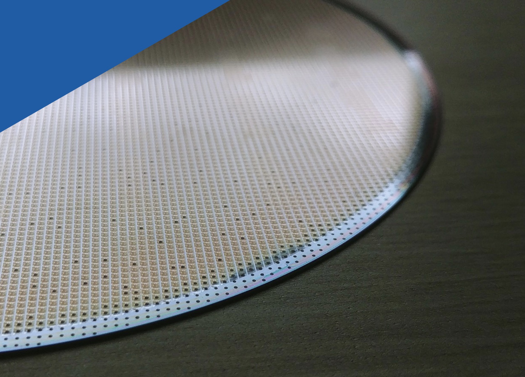
2D materials have been proven to enable superior device performance across a wide range of applications such as sensors and photonics. The next step needed to bring these devices to market is to develop the processing flow for full wafers. Oxford Instruments is ideally positioned to help take the technology to the next level with a clear roadmap to single wafer plasma processing solutions on 200 mm wafers.
Oxford Instruments has successfully installed its Atomfab remote plasma ALD system at AMO Aachen to support the manufacture of these devices on 200 mm wafers. The innovative plasma ALD system has demonstrated the capability to deposit high quality high-K materials onto 2D materials with no layer damage. Atomfab was designed specifically for high volume manufacturing with market leading throughput and cost of ownership for remote plasma ALD delivered on a single wafer processing platform handling wafers up to 200 mm diameter.
“The new ALD tool will help AMO and the 2D Experimental Pilot Line (2D-EPL) to move research on 2D materials to higher manufacturing readiness levels”, says AMO’s director Max Lemme. “We are not merely talking about yet another tool, but about a strategic partnership between AMO and Oxford Instruments, with a dedicated Oxford Instruments scientist embedded at AMO to intensify the research and development on 2D materials. This close collaboration is a beautiful example for AMO’s mission to pursue technology transfer through joint R&D projects with industrial partners.”
Klaas Wisniewski, strategic business development director at Oxford Instruments Plasma Technology comments: “The equipment demand for next generation material devices has reached a new level. What is required are high-performance and at the same time cost-efficient solutions - criteria that cannot always be easily reconciled and can therefore only be implemented with superior process technology.
"We are therefore very pleased that this pioneering pilot line with access to the world leading device manufacturers will take full advantage of our advanced Atomfab ALD technology. By working together in such world leading consortia, we continue to build on our strategy of enabling the manufacture of high-performance devices by investing in promising technologies such as 2D materials today.”
Cedric Huyghebaert, program manager for exploratory material and module integration at imec, and technical leader of the 2D-EPL project states: “Over the past decade, research has unearthed some unique properties of two-dimensional materials that show potential for solving some key performance bottlenecks for future electronic and photonic devices and sensors.
He added: “While there are many demonstrations of lab type prototype devices showing performances beyond the state-of-the-art, to bring these devices into the market we need to develop tool kits and BKMs for manufacturing of 2D materials which are compatible with the standards of semiconductor industry. Imec is leading the 2D experimental pilot line effort to build an industrial ecosystem needed to drive up technology readiness of 2D materials and we are looking forward to working with Oxford Instruments and other tool and material vendors in this consortium.”


