Loading...
News Article

Allos GaN-on-Si tech used for brain/machine interface

News

Collaboration with Toyohashi University of Technology develops nitride-based micro LED chips for novel in-vivo application

Hiroto Sekiguchi's team at Toyohashi University of Technology and Allos Semiconductors have collaborated to develop high efficiency nitride-based micro LED chips for novel in-vivo neutral application.

Since their evolution in the 1990s, nitride LEDs have made inroads into our daily lives, saving energy and enabling many new applications. They are known for their ubiquitous use in numerous illumination applications and the emerging micro LEDs are famous in particular for use in super large TVs or groundbreaking augmented reality displays as well as robust automotive displays.

Beyond the obvious illumination applications, nitride LEDs are also increasingly proving helpful in medical applications. For example, nitride LEDs emitting UV light are employed to fight viruses like COVID-19 by disinfecting surfaces.

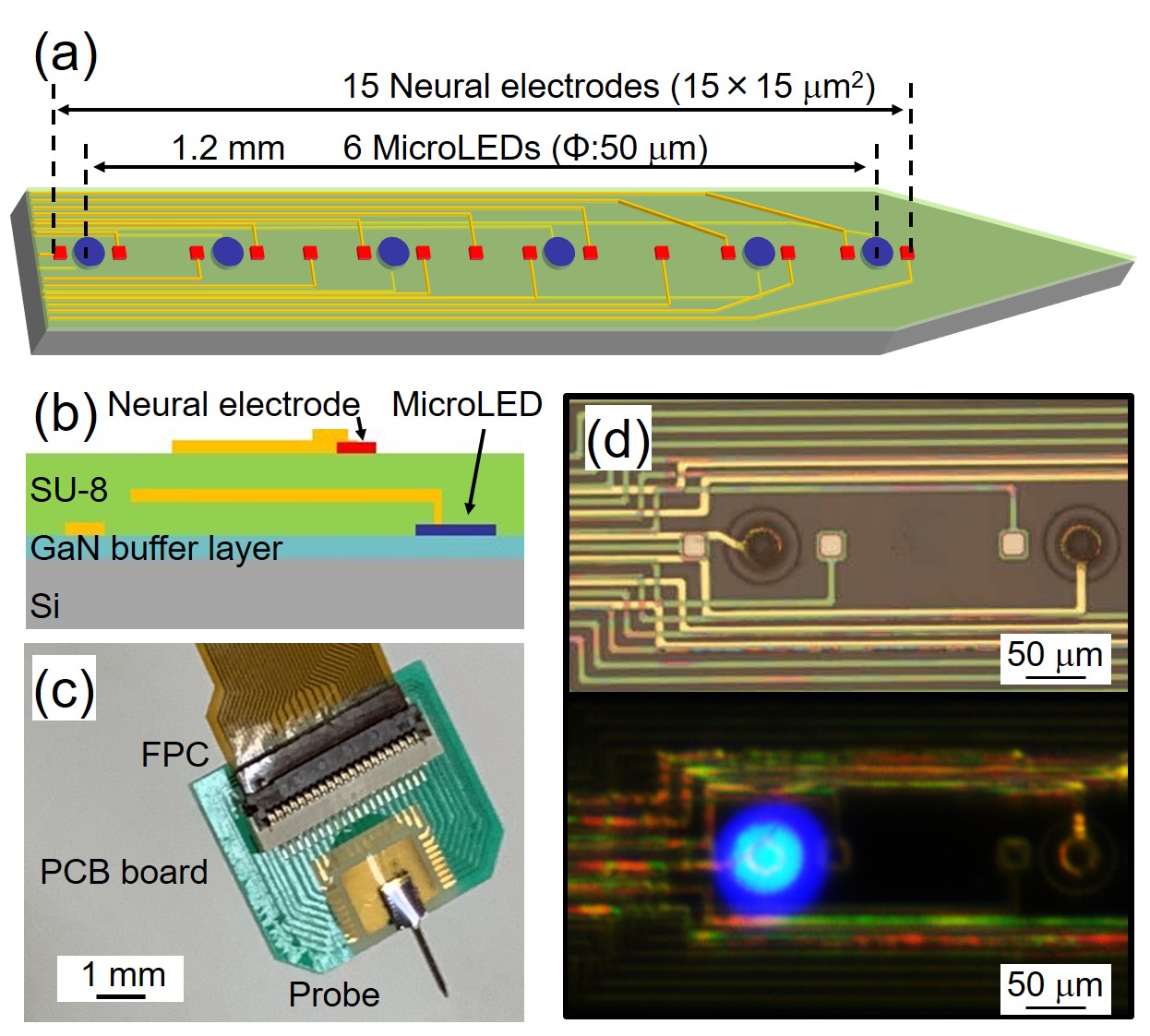
Another example is Toyohashi University of Technology, Japan using nitride micro LED technology to build medical brain/machine interfaces. Hiroto Sekiguchi’s group has developed a neural probe to study brain functions using Allos’ micro LED epiwafer. To avoid brain damage, high-efficiency of micro LEDs are key in order to reduce harmful impact from heat coming from conversion losses. Furthermore, for micro LEDs extreme precision is needed.

GaN-on-Si to overcome manufacturing challenges

For this novel medical application, manufacturing challenges had to been overcome, where Allos’ GaN-on-Si technology plays a key role. In particular, it was important to integrate nitride LED technology with mature and precise silicon industry processes in order to achieve highest accuracy and reliability standards.

Figure 1 above shows Micro LED neural electrode probe fabricated by Sekiguchi’s group integrating Allos’ high crystal quality and strain-engineering epiwafer technologies.

Commenting on the challenges, Sekiguchi said: “We need to achieve extreme precision and reliable results. Only industry-grade silicon processing equipment – as we fortunately have at our university – can deliver such processing results. Thus, using Allos’ GaN-on-Si epiwafers which can be processed on silicon lines was the right choice.”

Atsushi Nishikawa, CTO of Allos said: “With our CMOS line ready GaN-on-Si technologies we unlock the benefits those silicon lines bring – including scalability to 200 and 300 mm for low cost and the exceptionally high reliability and yield levels required for all micro LED applications.”

'Development of a neural probe integrated with high-efficiency MicroLEDs for in vivo application' by Hiroki Yasunaga et al; 'Applied Physics (Jpn. J. Appl. Phys. 60, 016503 (2021))

SPONSOR MESSAGE

Secure Your Hydrogen Supply

A study supply of high-purity hydrogen is critical to semiconductor fabrication. Supply chain interruptions are challenging manufacturers, leading to production slowdowns and stoppages. On-site hydrogen generation offers a scalable alternative for new and existing fabs, freeing the operator from dependence on delivered gas.

Plant managers understand the critical role that hydrogen plays in semiconductor fabrication. That important job includes crystal growth, carrier gas, wafer annealing, and in the emerging Extreme UV Lithography (EUV) that will enable new generations of devices. As the vast need for semiconductors grows across all sectors of world economies, so does the need for high-purity hydrogen.

Take control with Nel on-site hydrogen generation.

Read more
SiC MOSFETs: Understanding the benefits of plasma nitridation
Wolfspeed reports Q2 results
VueReal secures $40.5m to scale MicroSolid printing
Mitsubishi joins Horizon Europe's FLAGCHIP project
Vishay launches new high voltage SiC diodes
UK team leads diamond-FET breakthrough
GaN adoption at tipping point, says Infineon
BluGlass files tuneable GaN laser patents
QD company Quantum Science expands into new facility
Innoscience files lawsuit against Infineon
Riber revenues up 5% to €41.2m
Forvia Hella to use CoolSiC for next generation charging
Photon Design to exhibit QD simulation tool
Ortel transfers CW laser fabrication to Canada
Luminus adds red and blue multi-mode Lasers
PseudolithIC raises $6M for heterogeneous chiplet tech
Mesa sidewall design improves HV DUV LEDs
IQE revenue to exceed expectations
'Game-changing' VCSEL system targets clinical imaging
German start-up secures finance for SiC processing tech
Macom signs preliminaries for CHIPS Act funding
IQE and Quintessent partner on QD lasers for AI
EU funds perovskite tandems for fuel-free space propulsion
EU to invest €3m in GeSi quantum project
Transforming the current density of AlN Schottky barrier diodes
Turbocharging the GaN MOSFET with a HfO₂ gate
Wolfspeed launches Gen 4 SiC MOSFET technology
Report predicts high growth for UK's North East
Element Six unveils Cu-diamond composite
SemiQ launches hi-rel 1700V SiC MOSFETs
Lynred to exhibit Eyesential SWIR sensor for machine vision
Thorlabs buys VCSEL firm Praevium Research
×
Search the news archive

To close this popup you can press escape or click the close icon.
Logo
x
Logo
×
Register - Step 1

You may choose to subscribe to the Compound Semiconductor Magazine, the Compound Semiconductor Newsletter, or both. You may also request additional information if required, before submitting your application.


Please subscribe me to:


You chose the industry type of "Other"

Please enter the industry that you work in:
 
x
Adblocker Detected
Please consider unblocking adverts on this website