
Self-aligned growth spawns hybrid photonic devices
Miniature, high-performance optical links could be formed on silicon substrates through self-aligned growth in oxide tubes
BY SVENJA MAUTHE, NOELIA VICO TRIVIÑO, MARILYNE SOUSA, HEINZ SCHMID AND KIRSTEN MOSELUND FROM IBM RESEARCH EUROPE
SILICON MICROELECTRONICS has made staggering progress. The latest components have a footprint of just a few tens of square nanometres, consume very little power, and are packed in their billions on a chip.
Today’s technology, the culmination of decades of silicon CMOS processing development, has also spawned advances that benefit silicon photonics. Fabs can now produce low-loss silicon waveguides and passive structures to route optical signals through a chip. However, this technology is not perfect. Arguably its biggest weakness is the lack of optical gain, stemming from silicon’s indirect bandgap.
Free from this limitation are a portfolio of III-V compound semiconductors with direct bandgaps spanning the entire spectral range from the visible, using III-nitrides, to the near infrared (see Figure 1). The latter is of interest for optical communication, with bands around 1350 nm and 1550 nm – they are known as the O-band and C-band – providing the preferred choices for datacom and telecom, respectively. These bands have been adopted because they correspond to minimum transmission losses in optical fibres, and coincide with the availability of effective sources and erbium-doped fibre amplifiers (EDFAs). These spectral domains are also well suited for on-chip applications, thanks to silicon’s transparency at wavelengths beyond 1.1 μm. Due to this attribute, SOI waveguides can serve as a low-loss transmission medium.
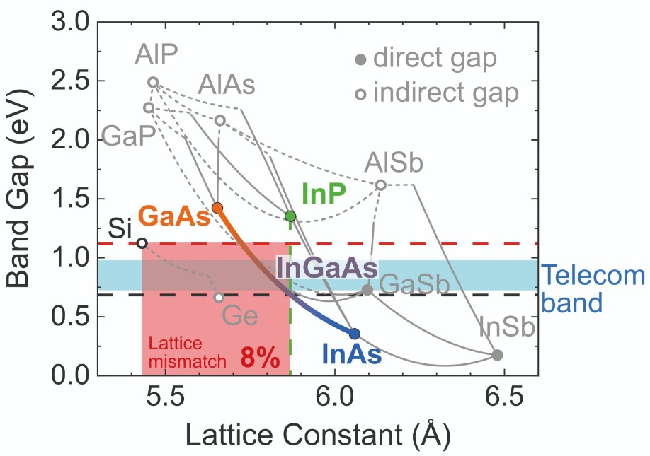
Figure 1. Bandgap versus lattice constant for a variety of direct (full circle) and indirect (circle) semiconductors. The 8 percent lattice mismatch between silicon and In0.53Ga0.47As is highlighted. The blue shaded area corresponds to the telecommunication band.
Uniting III-Vs and silicon
One of the holy grails of research within the semiconductor industry is the seamless integration of photonics and electronics, so engineers can draw on the best of both worlds. Today, the state-of-the-art approach to accomplishing this is to directly bond a wafer with a III-V active stack onto a pre-processed silicon wafer (see Table 1, which compares this approach to other techniques for integrating III-Vs on silicon). Wafer-bonding allows light to couple evanescently from underlying silicon waveguides to the active III-V regions above. Engineers have demonstrated highly advanced devices with this approach, integrating both detectors and lasers.
Bonding can also take place at the die level. In this case, individual III-V dies or pre-processed III-V devices can be united with a silicon platform. While these chips may seem small from the perspective of the III-V community, with dimensions of several hundred microns, they are far, far larger than electronic components. With transistors typically fitting within tens of nanometres, the size mismatch is about three orders of magnitude.
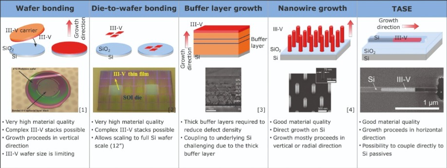
Table 1: Overview of existing technologies for integrating III-V materials on silicon. Reprinted with permission from [1] M. Seifried et al. IEEE JSTQE 24 8200709 (2018), doi: 10.1109/JSTQE.2018.2832654, licensed under CC BY 4.0; [2] S. Keyvaninia et al. Opt. Mater. Express 3 35 (2013), doi: 10.1364/OME.3.000035, ©2012 Optical Society of America; [3] I. Luxmoore et al. Sci Rep 3 1239 (2013), doi: 10.1038/srep01239, licensed under CC BY-NC-ND 3.0; [4] T. Katsuhiro et al. J. Phys. D: Appl. Phys. 47 394001 (2014), doi: 10.1088/0022- 3727/47/39/394001, ©2014 IOP Publishing Ltd, CC BY 3.0.
A well-known approach to overcoming both these issues is to switch from growing a stack of layers to growing nanowires. The growth of III-V nanowires can begin with a metal catalyst (usually vapor-liquid solid type growth), or with an opening defined in a pre-patterned hard-mask on the surface of a silicon wafer, and approach known as selective-area epitaxy.
Our team at IBM Europe has trailblazed yet another technique for marrying III-Vs with silicon. Our approach, which we refer to as template-assisted selective epitaxy (TASE), involves the growth of III-Vs within oxide tubes formed on a silicon substrate (see Figure 2 for an outline of the process flow).
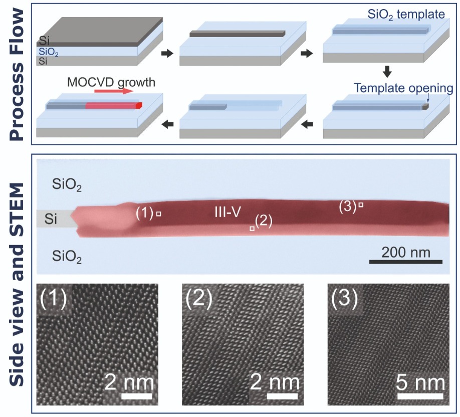
Figure 2. Template-assisted selective epitaxy (TASE) process flow and material investigation using scanning transmission electron microscopy (STEM). TASE is performed on an SOI wafer. The top silicon surface is patterned and covered with SiO2. Subsequently an opening is etched into the oxide shell on one side and the underlying silicon is partially etched. Using MOCVD, III-V material is grown from the remaining silicon into the empty SiO2 tube. Images reprinted with permission from S. Mauthe et al. Nat. Commun. 11 4565 (2020).
It is interesting to note, however, that we did not develop TASE for photonics. Initially, we targeted electronic applications, using this technology to provide a complementary tunnel FET platform, which is described on pages 38 to 42 of the January/February 2017 edition of Compound Semiconductor.
There are two essential attributes of our TASE technology that enable us to form the devices described in the remainder of this article. Firstly, because our method relies on replacing existing silicon features by a III-V, it is self-aligned – the shape and position of the compound semiconductor material that we add is defined in the same lithographic step as the silicon features. Thanks to this, we can perfectly tune the coupling to waveguides, and we can insert scaled III-V features within a silicon photonic crystal lattice. The upshot is that we engineer truly hybrid structures, integrated seamlessly. Secondly, we can introduce doping profiles and composition gradients in-situ, during growth. One of the merits of the geometry that results from our process is that it makes coupling to silicon waveguides straightforward.
Monolithic detectors
As optical signalling extends from server racks to on-board and finally on-chip schemes, demand for detectors will grow to thousands, if not millions. While an on-chip light source is highly desirable but not mandatory, densely integrated photodetectors are an essential ingredient in optical transceivers, required to process the incoming optical signal.
To successfully replace lossy electronic interconnects, it is critical that power-consumption is at the very least similar – and ideally lower – than that of comparable electronic interconnects. Efforts must focus on limiting RC constants, a requirement that can be accomplished with small-footprint devices with small capacitances. The key to satisfying these constraints is to transition away from today’s large, high-performance devices – and this is where III-Vs have an important role to play.
 Figure 3. Overview of electro-optical performance of a scaled, TASE-grown photodetector with 200 nm width. The top part of the image depicts a typical diode-like current-voltage (IV) curve on the left-hand side. Under light illumination, a photocurrent flows, increasing with illumination power. Plotting the measured current under reverse bias as a function of the incident light illumination reveals a linear relationship, suggesting a high responsivity (see middle image). On the right-hand side, the S21 response measurement is depicted. The line at -3 dB marks the 3-dB limit. The lower part depicts the high-speed data reception measurements. As illustrated, an optical fibre is aligned free-space and light modulated onto the device. The three images on the right depict the measured eye diagrams with open circles up to 32 Gbit/s. Images reprinted with permission from S. Mauthe et al. Nat. Commun. 11 4565 (2020).
Another reason for embracing the III-Vs is that SiGe compounds do not span an ideal absorption range. They make for excellent detectors in the visible, and can reach the O-band at around 1350 nm by increasing the germanium concentration, but the important 1550 nm wavelength is very close to the detection limit.
Recently, we demonstrated the first InGaAs photodetector that is monolithically integrated in-plane on silicon, growing the device from a silicon fin. From a photonics perspective, this might be viewed as a butt-coupling approach. We focused on improving speed and power efficiency through scaling. To this end, we kept geometries small, limiting height to only 60 nm. As this is insufficient for sustaining a propagating mode in the near-infrared, we turned to free-space fibre coupling for device characterisation.
Our devices exhibit impressive characteristics. Dark current is low, while estimated responsivity hits 0.65 A/W. As our free-space coupling prevents a direct measurement of responsivity, we calculated this value, assuming that only the photons absorbed in the intrinsic region contribute to the photocurrent, which is an ideal case scenario.
To demonstrate the potential of our technology for high-speed data transmission, we have recorded eye diagrams. They show that we can distinguish ‘0’ from ‘1’ at data rates up to 32 Gbit/s, the limit of our experimental setup. These results, illustrated in Figure 3, shows a f3dB of about 25 GHz in the frequency response curve. While these results are encouraging, even better ones should follow. Opportunities for further progress include introducing an improved contact and layout scheme and optimising the resistive components of the devices.
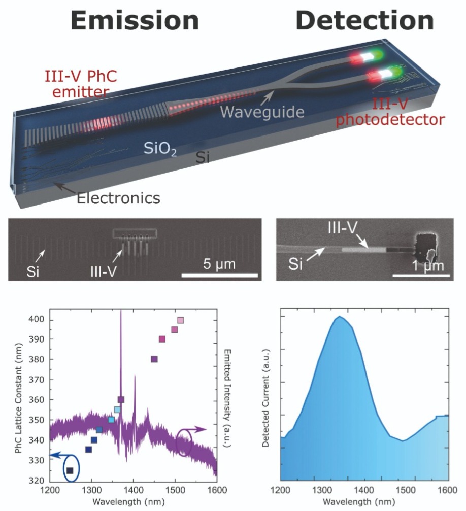
Figure 4. Vision of a TASE platform for integrated optical links. The top image shows the envisioned optical link with a photonic crystal (PhC) cavity emitting light directly into a waveguide. The waveguide is coupled to detectors to detect the emitted light. In the centre, two scanning electron microscopy images depict a fabricated photonic crystal cavity and a photodetector, respectively. The bottom two images depict the spectral performance of the emitter and detector, respectively. The images are reprinted with permission from S. Mauthe et al. Nat. Commun. 11 4565 (2020) and S. Mauthe et al. Nano Lett. 20 8768 (2020).
Hybrid photonic crystals
Our ultimate goal is to fabricate a fully integrated optical link. To realise this, we need to develop an on-chip laser or emitter. We are pursuing a photonic crystal architecture. This is a promising option for anin-plane light source, because it has the potential to combine high efficiency with low power and miniaturisation, thanks to a high quality factor and a small mode volume.
Most photonic crystal structures are two-dimensional or one-dimensional lattices, created by etching holes in a dielectric material or by stacking densely placed rods or fins. The latter architecture can be directly integrated with our TASE technology, which we developed for the detectors. Following in the footsteps of our process for making detectors, we etch back the silicon in a selected number of rods, prior to re-growth of the III-V. This is a straightforward approach to creating a hybrid structure, where most of the photonic crystal cavity consists of plain silicon – III-V is only present in the central region of the cavity.
With this design, the InGaAs emits in the near-infrared, above the silicon absorption edge. At this wavelength the silicon part of the photonic crystal cavity is transparent. By only using gain material where essential, we trim optical losses, leading to a substantial improvement in the final device performance. It is a non-trivial task to design a photonic crystal structure with a high quality factor. Helping with this endeavour, we recycle existing designs, replacing just an important segment of the cavity with III-V while retaining the remaining features in silicon.
Our hybrid photonic devices produce tuneable light emission across the telecommunication band. They offer many valuable characteristics: they feature high yield and robustness, with similar experimental Q-factors in excess of 1000; and controllable cavity emission wavelengths, despite some fabrication imperfections. We attribute their strengths to the hybrid concept, which at its heart has the placement of III-Vs at just the desired locations within the photonic crystal silicon structure.
The individual III-V photodetectors and optically pumped photonic crystal light sources that we have demonstrated provide great stepping stones towards our long-term goal of a fully integrated optical link. Our efforts are now being directed at developing a larger waveguide-coupled version of our detector that will allow direct on-chip coupling to integrated lasers. If our optical link is to make an impact, it must also feature light sources that are electrically actuated, rather than optically pumped. That is an extremely challenging requirement for miniature devices – so-called nanolasers or nanoLEDs – as the presence of metals in the vicinity of the optical mode invariably leads to losses, and this inevitably increases the threshold.
We believe that our in-situ, in-plane doping process holds the key to producing tiny, electrically pumped emitters. We have already embedded the appropriate composition and doping profile in the III-V rods, and our next step is to add contacts to the ends of these rods, to enable electrical actuation. However, while the next step is clear, implementation is going to be challenging. We can expect a fair bit of engineering to optimise design and accurately integrate low-resistance electrical contacts without destroying the optical mode.
In some ways, the use of TASE is a paradigm shift in the design of nanophotonic devices. Like any new technology, there are challenges – but there are also completely new opportunities, just waiting to be explored.
This work received financial support from European Research Council ERC StG PLASMIC under grant agreement no. 678567 and from Swiss National Science Foundation SNF Spark under grant agreement CRSK-2_190806.
H. Schmid et al. Appl. Phys. Lett. 106 233101 (2015)
S. Mauthe et al. Nat. Commun. 11 4565 (2020)
S. Mauthe et al. Nano Lett. 20 8768 (2020)
S. Matsuo et al., Nat. Photonics 4 648 (2010) doi:10.1038/nphoton.2010.177


