
New nanowires spawn superior UV LEDs
Switching from AlGaN nanowires to those made from AlInN offers an attractive route to increasing the output of the UV LED
BY RAVI TEJA VELPULA, BARSHA JAIN, AND HIEU PHAM TRUNG NGUYEN FROM NEW JERSEY INSTITUTE OF TECHNOLOGY
The outbreak of the deadly SARS-COV-2 virus has thrown the UV source into the spotlight. Those emitting deep within the UV, in a domain stretching from 222 nm to 207 nm, can kill this virus and many others, and also deliver surface disinfection. In addition, there are related applications for deep UV radiation, such as water disinfection, that use this source to disrupt DNA and RNA molecules.
As well as this class of application, UV sources can take on many other important tasks: they can be employed for a wide range of UV curing applications, including those involving coatings, inks, adhesives, composites, and stereolithography; they can be used to solicit photochemical reactions in living organisms; and they provide an option for treating several skin diseases, such as psoriasis, vitiligo, and cutaneous T-cell lymphoma.

Figure 1. Applications of light-emitters in the UV. Radiation is generally divided into three spectral bands, based on specific wavelengths: UVA (400 nm-320 nm), UVB (320 nm-280 nm), and UVC (280 nm-100 nm).
Thanks to these strengths, market analysts expect sales of the UV LED to climb in the coming years. Yole Développement predicts global revenue to increase from $320 million in 2020 to $1 billion in 2023, while Allied Market Research forecasts a compound annual growth rate of 21 percent over the next few years that will propel the value of this market to $1.7 billion by 2027.
Yet despite all this promise and expectation, the UV LED has its faults. Chief amongst them is a low efficiency, which plummets as the emission wavelength heads deeper into the UV. The efficiencies of these AlGaN-based devices are in single digits, held back by a number of factors that include a high density of dislocations, induced polarization fields, electron leakage, poor p-type doping, inefficient hole transportation, substantial internal absorption, a high internal total reflection, and a dominant transverse magnetic mode that drags down the light extraction efficiency. Despite much effort to improve both the internal quantum efficiency and the light extraction efficiency, the external quantum efficiency – the product of those two factors – is still low in planar AlGaN UV LEDs.
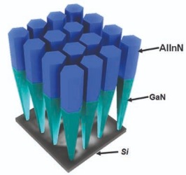
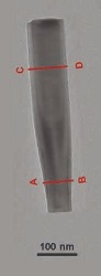
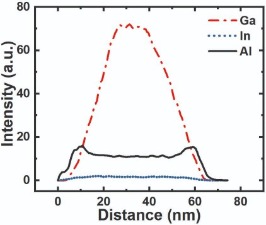
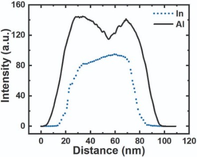
Figure 2. (a) AlInN/GaN nanowires can be grown on silicon substrates (b) A transmission electron microscopy image of the AlInN/GaN nanowire, clearly showing the presence of a core-shell structure. Energy dispersive X-ray spectrometry line scan profile showing (c) the quantitative variation in gallium, indium and aluminium signals along lines A-B, and (d) variation in the indium and aluminium signal along lines C-D (Adopted from R. T. Velpula et al. Sci. Rep. 10 2547 (2020)).
AlGaN or AlInN
One promising pathway to improving the performance of the UV LED is to switch from AlGaN nanowires to those made from AlInN. The latter is relatively unexplored, but holds great potential for UV and visible LEDs. Strengths of this ternary include lattice-matching to GaN with an indium content for AlInN of around 17-18 percent, and a high refractive index contrast with GaN.
In addition, AlInN compounds can be grown on both GaN and AlN templates – note that AlGaN is inimical to grow on GaN templates – and compared to AlGaN, AlInN offers wider windows of optimal alloy composition, especially in the deep UV.
Despite these tremendous advantages, progress with AlInN has been slow. Hampering efforts has been the immature epitaxial growth of high-quality AlInN. When grown by MBE, there tends to be significant compositional inhomogeneity, probably rooted in the extremely large differences in the optimal growth temperatures of the two ‘components’ – for InN, growth should take place at around 450 °C, while for AlN it needs to be in the region of 800 °C.
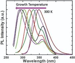
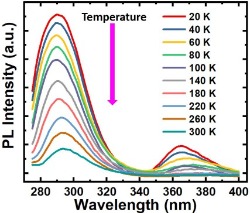
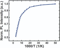
Figure 3. (a) Photoluminescence spectra of AlInN/GaN nanowires. Peak emission varies from 290 nm to 355 nm. (b) Temperature-dependent photoluminescence intensity of AlInN/GaN nanowires measured from 20 K to 300 K. (c) Photoluminescence intensities of AlInN/GaN nanowires under different temperature conditions (adopted from R. T. Velpula et al. Sci. Rep. 10 2547 (2020)).
We have produced our vertically aligned, self-organized AlInN/GaN core-shell nanowires on n-type silicon (111) substrates using an RF plasma-assisted Veeco Gen II MBE tool (see Figure 2 (a)). Epitaxial conditions for our GaN nanowires include a growth temperature of 770 °C, a nitrogen flow rate of 1.0 sccm, a forward plasma power of 400 W, and a gallium beam equivalent pressure of 6 × 10⁻⁸ Torr. After growth of the GaN nanowires, we add self-organized AlInN segments that provide UV light emission. By varying the indium and aluminium beam flux and/or the substrate temperature, we control the composition of the active region.
Scanning transmission electron microscopy has enabled the characterisation of the structural properties of our AlInN/GaN nanowires. This technique uncovers the presence of GaN and AlInN segments (see Figures 2(b)-(d)) and reveals that the wire diameter increased from the GaN segment to the AlInN portion and remained constant on the top of the nanowire. Our images also suggest that a core-shell AlInN/GaN structure spontaneously formed during epitaxial growth of the AlInN layer. If that’s the case, this is an asset, because a core-shell structure offers strong carrier confinement and reduced non-radiative recombination on the nanowire surface, leading to enhanced optical characteristics.
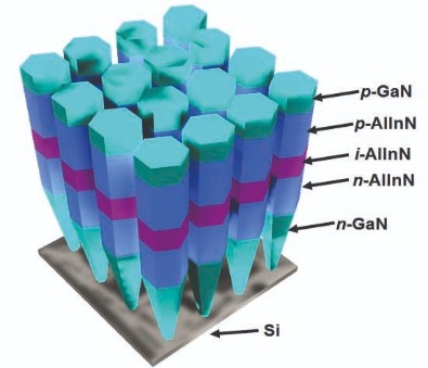
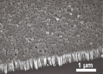
Figure 4. (a) A silicon substrate provides a platform for a p-i-n AlInN nanowire LED structure. The devices contain a layer of GaN:Si that is about 200 nm-thick, as well as 100 nm AlxIn1-xN:Si/40 nm i-AlyIn1-yN/100 nm AlxIn1-xN:Mg, and 10 nm GaN:Mg (b) 45o tilted scanning electron microscopy image of p-i-n AlInN nanowire LED sample (adapted from R. T. Velpula et al. Sci. Rep. 10 2547 (2020)).
A more thorough investigation has been undertaken for AlInN nanowires produced with a growth temperature of 710 °C. These wires have a strong emission at 295 nm, with an associated spectral linewidth of 28 nm. Using 10 mW excitation, we have measured the photoluminescence at a variety of temperatures between 20 K and 300 K (see Figure 3(b)). This provided an estimate of the internal quantum efficiency, calculated by comparing the integrated photoluminescence intensities of emission from the AlInN layer at room temperature and at 20 K, and assuming that the internal quantum efficiency at 20 K is close to unity. This approach suggests that the room-temperature internal quantum efficiency of the AlInN/GaN nanowires is 52 percent (see Figure 3 (c)). We attribute this relatively high value to the strong carrier confinement provided by the AlInN shell and the nearly intrinsic AlInN core.

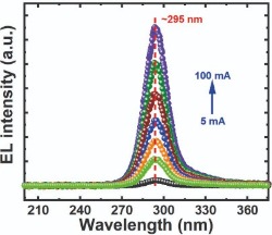
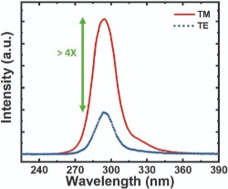
Figure 5. (a) Current-voltage characteristics of the AlInN UV nanowire LED. The inset shows the current-voltage plot for the AlInN UV LED on a semi-log scale. (b) Electroluminescence spectra of the AlInN UV nanowire LED. (c) The transverse-magnetic (solid line) and transverse-electric (dotted line) polarized spectra of the AlInN UV nanowire (adopted from R. T. Velpula et al. Sci. Rep. 10 2547 (2020)).
Fabrication of our devices begins by cleaning the epiwafers in HCI and then HF. These steps remove the oxide layer from the backside of the silicon substrates and native oxides from the nanowire surface. We then create a n-contact on the backside of the silicon by depositing a metal stack, comprising 20 nm of titanium and 120 nm of gold; and turn to electron-beam evaporation to create a p-metal contact by depositing 10 nm of nickel and 10 nm of gold. After this, we add 20 nm of nickel and 120 nm of gold, on top of the device, to serve as a metal pad. We anneal the resulting structure at around 550 °C for 1 minute to achieve low contact resistance.
Our AlInN LEDs exhibit excellent current-voltage characteristics, combining a low resistance at room temperature with a turn-on voltage of about 5 V, a value that is at least as good as that of AlGaN UV LEDs operating in this spectral domain (see Figure 5 (a)). These devices produce strong UV light emission at around 295 nm at injection currents from 5 mA to 100 mA (see Figure 5 (b)).
The particular polarization of the light generated within the UV LEDs can govern the output of this device. Using a 10 A cm-2 injection current, we have investigated the polarization of our devices, defining the transverse-magnetic and transverse-electric directions as those with electric fields parallel and perpendicular to the c-axis, respectively. These measurements reveal that the light emission in our devices is predominantly transverse-magnetic polarized – this signal is more than four times that of the transverse-electric mode (see Figure 5 (c)).
To enhance light extraction through optimisation of polarization, we have considered the morphology of our devices. This theoretical study considered photonic crystal structures with randomly grown, square, and hexagonal lattices (see Figure 6).
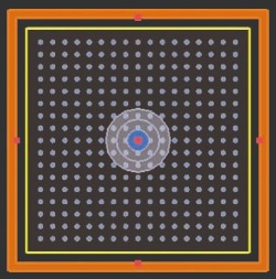
Figure 6. Top view of random array (left), square array (middle), and hexagonal array (right) of AlInN nanowire UV LEDs (adopted from B. Jain et al. Opt. Exp. 28 22908 (2020)).
Our calculations show that the maximum light-extraction efficiency for the square array is 56 percent, realised with a spacing of 195 nm and a radius of 40 nm. Better results are possible with hexagonal nanowires, with light extraction efficiency hitting 63 percent for a spacing of 230 nm and a radius of 60 nm. These results underscore the critical role that geometry plays in directing the generated photons from the active region to air.
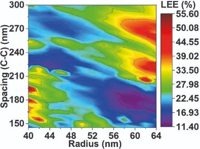
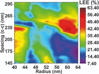
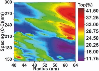
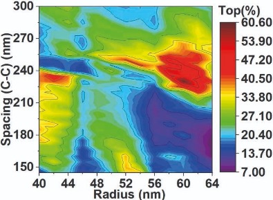
Figure 7. Contour plot of the light-extraction efficiency for a differing nanowire radius and spacing for a square array (a) and a hexagonal array (b) of AlInN nanowire UV LEDs. Contour plot of the light-extraction efficiency from the top, for a differing nanowire radius and spacing for the (c) square array and (d) hexagonal array of AlInN nanowire UV LEDs (adopted from B. Jain et al. Opt. Exp. 28 22908 (2020)).
Our work, involving the introduction of the world’s first axial AlInN core-shell nanowire UV LEDs, offers a new pathway for producing sources in this spectral range. Devices are in their infancy, and performance is sure to improve through optimising the LED structure, nanowire morphology, diameter and spacing. They are long-term goals for us, but our efforts will initially head in a different direction, reducing emission wavelengths to below 230 nm, so that these LEDs can serve in air and surface disinfection.
R. T. Velpula et al. Scientific Reports 10 2547 (2020)
B. Jain et al. Opt. Exp. 28 22908 (2020)
R. T. Velpula et al. Optical Materials Express 10 472 (2020)
R. T. Velpula et al. CLEO: Science and Innovations (pp. STu3P-4). Optical Society of America, 2020.


