
Nano-porous GaN enhances microLEDs

Inserting quantum dots in nanopores creates efficient, reliable microLEDs.
BY JIE SONG AND CHEN CHEN FROM SAPHLUX
DISPLAYS MADE from microLEDs are attracting tremendous attention due to their long lifetime, high brightness and excellent efficiency. Helping to put them in the spotlight are some of the biggest tech companies in the world, such as Apple and Samsung, which are developing this form of display using mass-transfer or nanoprint technology.
Despite years of intense development, several key technical issues are still hampering the key ingredient, the miniaturised LED. Those emitting in the red are plagued by a low efficiency and a thermal droop, limiting the performance of the display; it is challenging to fabricate devices with a pitch below 10 µm, a requirement for microdisplays for augmented reality and mixed reality; as the size of the LED reduces, bin sorting gets harder and more costly; and of greatest concern of all, production costs are high.
Helping to address all these issues are colour-converted microLEDs, which use a chip emitting in the ultraviolet or blue part of the spectrum to pump quantum dots. Devices that operate in this manner have many unique properties, including a high quantum yield, a size-dependent emission wavelength, a narrow emission linewidth, and a short luminescent lifetime. What’s more, by using patterning and spin-coating to add quantum dots to the substrate, this class of LED can serve a broad range of applications.
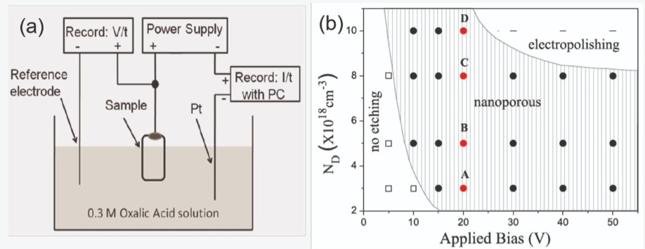
Figure 1. (a) An electrochemical etching process produces nano-porous GaN. (b) A phase diagram of the GaN electrochemical etching process shows how the etching characteristics are related to silicon doping in GaN and the applied bias.
To address these issues, our team from Saphlux of Branford, Connecticut, has developed a nano-pore technology that allows quantum dots to be embedded in microLEDs. This results in devices that are very efficient, reliable, and low in cost.
Nano-porous GaN
We create nanoscale pores in our LEDs by dipping the material in an acidic solution and applying a bias, which drives electro-chemical etching of n-type GaN (see Figure 1 (a)). By varying either the applied bias voltage or the silicon doping concentration in GaN, we are capable of producing dramatic changes in electro-chemical etching behaviour. If we apply a low bias voltage to GaN with a low silicon-doping concentration there is no etching; and if we use a high bias voltage or a high silicon-doping concentration, we etch GaN completely away (this is called electropolishing). To form nano-porous GaN we chart a course between these extremes, selecting an appropriate bias voltage and silicon doping concentration.
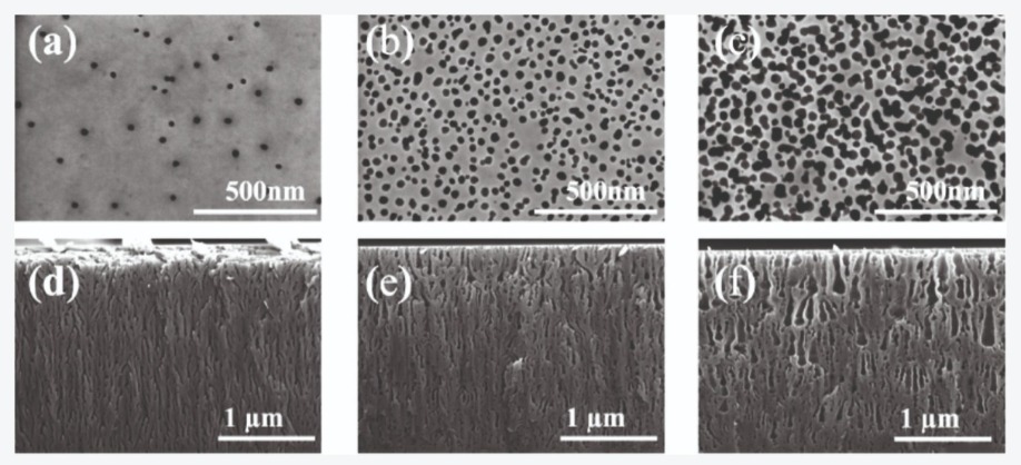
Figure 2. (a-c) Top-view and (d-f) cross-sectional scanning-electron microscopy images of nano-porous GaN with different porosity etched at different bias voltages. Reprinted with the permission of the American Society Chemistry.
Simulations suggest that the incorporation of nanopores into our LEDs can lead to a tremendous increase in device efficiency. For planar quantum dots in a polymer film, light-conversion efficiency increases linearly with increases in the thickness of the quantum dot layer to a maximum of only 20 percent – that’s for a 10 µm-thick quantum-dot layer (see Figure 3(a)). In stark contrast, when dots fill the nanopores, light-conversion efficiency exceeds 80 percent, for a film thickness of just 5 µm.
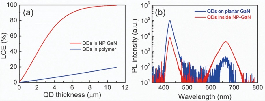
Figure 3. (a) Simulated results for the light-conversion efficiency (LCE) of quantum dots (QDs) loaded in polymer and nano-porous GaN, respectively. The same concentration of dots is used in both samples. (b) Photo-luminescence spectra of red QDs on planar GaN and nano-porous GaN, respectively.
Benefits of the nano-porous structure are not limited to greater efficiency. Reliability also increases, as demonstrated by our optical excitation measurements at a high power density. When we pumped the planar samples with a 420 nm blue laser at an optical power density of about 25 W cm-2, the normalized intensity of red emission fell to just 20 percent of its initial value after 3 hours of excitation. In comparison, when dots were housed in the nano-pores, identical excitation conditions led to a 55 percent reduction in intensity compared with the initial value.
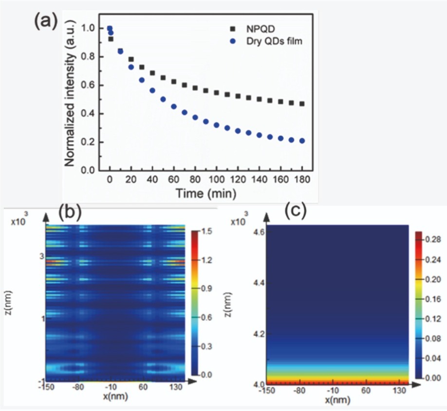
Figure 4. (a) Comparison of the normalized power intensity of red emission from a red nano-porous quantum-dot sample and a quantum-dot film on a GaN-on-sapphire wafer. Both samples were subjected to 3 hours of excitation with a 420 nm blue laser. (b) Simulated mapping results of blue light absorption by nano-porous GaN. (c) Simulated mapping results of blue light absorption by a nano-porous film.
Dots for displays
Producing our displays involves forming nano-porous blue-emitting LEDs, before putting some of them aside and coating others with either red-emitting or green-emitting dots (see Figure 5). We bond exposed nano-porous GaN to a current driver panel, before loading red- and green-emitting dots onto different zones. If the zones are free from dots, they emit blue light; and if they are loaded with dots, they produce red or green emission through colour-conversion.
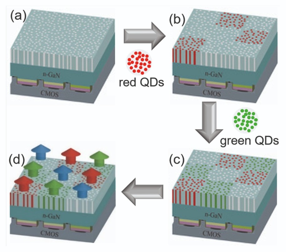
Figure 5. Saphlux’s approach to making monolithic RGB microLEDs. (a) A vertical blue LED with exposed nano-porous GaN is bonded to a current-driver panel. (b) Red quantum dots are selectively loaded into red zones. (c) Green quantum dots are selectively loaded into green zones. (d) Red, green and blue light emitted from red quantum dot zones, green quantum dots zones, and zones without any quantum dots, respectively.
We are now fabricating nano-porous GaN microLED arrays with customized pixel sizes to suit the needs of our customers. Many applications offer broad market prospects, including wearable devices, vehicle displays, smartphones, and various forms of augmented and virtual reality.
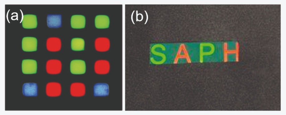
Figure 6. (a) Saphlux RGB monolithic microLEDs excited by a blue LED source from the backside. (b) A picture of the company logo “SAPHLUX” fabricated by red and green nano-porous quantum-dot microLEDs.
These devices, like their smaller siblings, show much promise. They are well-positioned to drive the manufacture of displays made from tiny, efficient, reliable LEDs that are low in cost and will help this market to blossom.
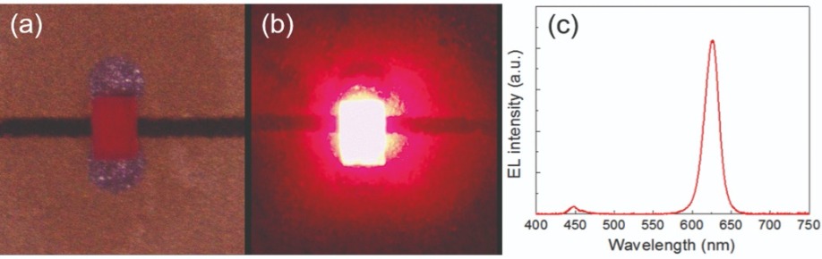
Figure 7. Photos of 100 × 150 µm2 red nano-porous quantum dot miniLED mounted on a PCB board (a) and lit-up at an injection current of 1 mA (b). (c) Spectrum of a red nano-porous quantum dot LED shown in (b). Testing the reliability of the red nano-porous quantum-dot miniLED revealed acceptable results at 30 W cm-2. This power density is more than sufficient for most microLED applications.
D. Peng et al. J. Disp. Technol. 12 742 (2016)
H.-V. Han et al. Opt. Express 23 32504 (2015)
J.-H. Kang et al. ACS Appl. Mater. Interfaces 12 30890 (2020)
C.-T. Lee Cheng et al. IEEE Photonics Technol. Lett. 27 2296 (2015)
K.-B. Bae Lee et al. Phys. Status Solidi A 215 1700644 (2018)
E. Jang et al. Adv. Mater. 22 3076 (2010)


