
Disrupting the tubes market with high-voltage GaN HEMTs
GaN HEMTs operating at voltages of up to 150 V outperform vacuum tubes by combining high performance with greater reliability, longer lifetime and lower operating costs
BY GABRIELE FORMICONE, JEFF BURGER, JAMES CUSTER AND JOHN WALKER FROM INTEGRA TECHNOLOGIES
INVENTED PREDOMINANTLY in the first half of the twentieth century, vacuum electron devices (VEDs) have a long history as a critical component enabling satellite communications, radar systems, high-energy particle accelerators, and other applications requiring high output power, wide operating bandwidth and high efficiency. VEDs include traveling-wave tubes and klystrons.
While VEDs are an accepted technology, they suffer from multiple weaknesses, many of which can be addressed by semiconductor-based solid-state amplifiers, which have become the mainstream technology in the lower power, lower frequency VED market. Semiconductor-based solutions deliver longer lifetime, superior ruggedness, and higher reliability, and reduce overall system size, weight, and costs. Yet despite all this success, solid-state sources have yet to penetrate the high end of the market for high power, multi-kilowatt applications.
Modernization of high-power RF communication and data transmission systems will push the requirements of what traditional VEDs can deliver. In addition, system architects are demanding more efficient power sources to meet green requirements while driving down operating costs over the system life. Thanks to the pioneering work of our team at Integra Technologies Inc., a market leader in RF and microwave high power devices, we have achieved a breakthrough by pushing the operating voltage for this class of device to a new high, raising the bar for high efficiency GaN-on-SiC technology. These efforts draw on our long heritage of silicon bipolar and GaN/SiC RF high power expertise at 28 V and 50 V, with our latest success representing yet another milestone in our advancements in green technology, which date back to 2013. The ground-breaking progress that we have made enables high-voltage GaN/SiC-based HEMTs to offer a compelling commercial alternative to the VED.

Figure 1. Measured RF power gain and drain efficiency versus output power at 145 V bias and 400.8 MHz. Quiescent current is 100 mA. 6 Ω series gate resistors help to stabilise the transistor with 20 dB gain at 2 dB compression and 2.3 kW saturated power. Drain efficiency peaks at 80 percent. In CW operation at 100 V bias, saturated power is 1.2 kW with the same 80 percent peak drain efficiency.
Leveraging this field-proven IP, we have developed new epitaxial structures specifically designed for high-voltage operation. In addition to this advance, we have introduced and then patented innovated circuit and thermal management techniques specifically for high power operation. Benefiting from all this progress, our devices can now operate at voltages of up to 150 V, resulting in a dramatic improvement in output characteristics.
Our latest generation of high-voltage GaN/SiC devices, which produce pulsed power densities up to more than 20 W/mm, enables the production of solid-state devices with an output power of several kilowatts. Critical to the performance of the next high-power-generation green platforms, our HEMTs deliver sufficient gain, efficiency, and reliability to enable these systems to fulfil their performance targets.
Our devices are manufactured in a mainstream wafer fabrication foundry, using commercially available, production-ready materials.
Increasing power and dynamic range
At last year’s International Microwave Symposium, our company demonstrated the incredibly high output powers that can be produced by RF GaN/SiC transistors operating at elevated voltages of between 100 V and 150 V. We reported 2 x 50 mm gate periphery die yielding 1.2 kW when operating in CW mode at 100 V, and producing 2.3 kW when driven at 145 V using 100 µs-wide pulses and a 5 percent duty cycle. Plots of power gain and drain efficiency versus output power for these devices, which have a drain efficiency of 80 percent when operating in both modes, are shown in Figure 1. Two key features of this amplifier’s design are harmonic tuning, used to realise high efficiency, and patented thermal enhancement techniques that help mitigate heat dissipation in such high-power density transistors. We have designed the devices and circuits to operate at 400.8 MHz. This is the frequency employed in today’s largest particle accelerators, and also a frequency of interest for long-range, early-warning radar systems.
Our technology enables a single transistor to produce a CW power level of 2 kW and a pulsed output of 4 kW at an efficiency greater than 70 percent. With this level of performance, megawatt power levels can be realised with fewer combiners and lower related losses. By comparison, off-the-shelf 50 V RF technology would require massive power combiners to achieve similar performance, degrading system efficiency, while increasing the complexity of heat extraction. We also showcased the design flexibility of this technology by increasing the operating voltage to 150 V at the 2020 European Microwave Week. In this forum, we reported a single 50 mm gate periphery die that produced a 3 dB power dynamic range when modulating its operating bias from 100 V to 125 V and then on to 145 V (see Figure 2).
This amplifier’s devices and circuits are designed to operate at 325 MHz, targeting large particle accelerators. Our single semiconductor die delivers a 1.1 kW peak power at 145 V with 80 percent peak efficiency. The peak power decreases by about 3 dB at 100 V bias.
Going to even lower voltages can offer additional benefits. When we dial back the bias to 50 V, peak power can be modulated by around 6 dB while still preserving 80 percent peak efficiency; and we can realise additional dB of dynamic range by reducing the operating bias towards 28 V or 32 V. We have obtained similar results, also announced at European Microwave Week, with a power amplifier designed to operate at 650 MHz.
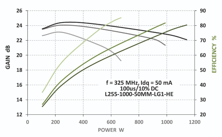
Figure 2. Measured RF power gain and drain efficiency versus output power for a 50 mm die with a signal of 100 µs pulse width and 10 percent duty cycle at 325 MHz. The device is characterized at 100 V, 125 V and 145 V DC bias demonstrating a 3 dB power dynamic range. By reducing operating bias to 50 V a 6 dB dynamic range is achieved.
Our R&D activities have extended to considering the bandwidth associated with the higher power densities and higher load impedances at 100 V and 150 V. Power-over-bandwidth is a ‘hot button’ in several applications, with requirements that may be strictly application-specific and not discussed in the public domain. What we can say, nonetheless, is that broadband high-power applications are destined to reap huge benefits from our 100 – 150 V amplifier technology.
System-level benefits
As mentioned earlier in this article, the higher voltage GaN transistors can achieve power densities of more than 20 W/mm, thus allowing for reduced circuit complexity for the same relative power level. As an example, two 1 kW transistors running at 50 V could be replaced by a single 2 kW transistor operating at 100 V. This eliminates one transistor and the combining structure required for the lower voltage solution.
Another advantage of a higher voltage is evident in a simple load-line analysis. While a 50 V device will provide a 25 W output power with just a 50 Ω load, a 100 V device will provide four times this power.
For broadband applications, higher voltage GaN HEMTs can also be an advantage, considering that the device impedances increase with higher voltage operation and the capacitance-per-Watt are reduced.
Lower voltage solutions require larger impedance transformations to achieve bandwidth, while a higher voltage solution can eliminate these transformers or reduce transformation ratios and their complexity. When utilizing 100 V GaN, the matching structure size can be reduced by a factor of two or more by removing transformers over a 50 V GaN solution for the same RF output power.
There is no doubt that much is to be gained from increasing the operating voltage of the GaN HEMT. There are benefits for the device itself, including an increase in output power, plus plenty of advantages at the circuit and system level. Our company is in talks with several VED’s users to commercialize our high-voltage GaN/SiC green technology.


