Loading...
News Article

GaN Systems launches Smallest 100W Charger Ref Design

News

Turnkey reference enables rapid design and rollout of smaller and more powerful and efficient GaN chargers

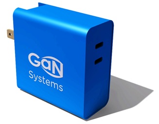
GaN Systems has announced the release of what it says is the industry’s smallest 100W dual USB-C intelligent PD GaN charger.

This turnkey reference design is said to achieve the highest power density of any 100W charger on the market. The charger can balance and appropriately power a variety of plugged-in device power level combinations from a single 100W device, two devices at 65W and 30W, or two 45W or 30W devices.

Additionally, when the power draw is below a certain threshold, the charger shifts to a higher efficiency mode to further maximise performance and reduce energy loss.

Available now through GaN Systems, the charger reference design includes prototypes and documentation (schematics, PCB layout, BOM, and design guideline) to shorten design cycles and speed up product launches.

The 100W charger reference design uses GaN Systems’ GS-065-011-1-L transistor. Key features include: high-power density of greater than 16W/in3 with case and foldable prong; dual USB-C ports to support universal USB-C protocols and flexible plug-in end devices; peak efficiency of over > 92.5 percent.

The design exceeds EN55032 Class B with > 6dB margin, meets safety IEC62368-1 touch temperature requirement, and meets IEC61000-3-2 for power line harmonics with Power Factor Correction (PFC) circuit.

“Consumers have spoken, and they want GaN chargers. 65 watts was the start and now everyone wants 100 watts and multiple ports,” says Jim Witham CEO of GaN Systems, “Our design, validated by leading customers, is the highest performance, smartest, and smallest charger design that gets customers’ products to market in record time.”

SiC MOSFETs: Understanding the benefits of plasma nitridation
Wolfspeed reports Q2 results
VueReal secures $40.5m to scale MicroSolid printing
Mitsubishi joins Horizon Europe's FLAGCHIP project
Vishay launches new high voltage SiC diodes
UK team leads diamond-FET breakthrough
GaN adoption at tipping point, says Infineon
BluGlass files tuneable GaN laser patents
QD company Quantum Science expands into new facility
Innoscience files lawsuit against Infineon
Riber revenues up 5% to €41.2m
Forvia Hella to use CoolSiC for next generation charging
Photon Design to exhibit QD simulation tool
Ortel transfers CW laser fabrication to Canada
Luminus adds red and blue multi-mode Lasers
PseudolithIC raises $6M for heterogeneous chiplet tech
Mesa sidewall design improves HV DUV LEDs
IQE revenue to exceed expectations
'Game-changing' VCSEL system targets clinical imaging
German start-up secures finance for SiC processing tech
Macom signs preliminaries for CHIPS Act funding
IQE and Quintessent partner on QD lasers for AI
EU funds perovskite tandems for fuel-free space propulsion
EU to invest €3m in GeSi quantum project
Transforming the current density of AlN Schottky barrier diodes
Turbocharging the GaN MOSFET with a HfO₂ gate
Wolfspeed launches Gen 4 SiC MOSFET technology
Report predicts high growth for UK's North East
Element Six unveils Cu-diamond composite
SemiQ launches hi-rel 1700V SiC MOSFETs
Lynred to exhibit Eyesential SWIR sensor for machine vision
Thorlabs buys VCSEL firm Praevium Research
×
Search the news archive

To close this popup you can press escape or click the close icon.
Logo
x
Logo
×
Register - Step 1

You may choose to subscribe to the Compound Semiconductor Magazine, the Compound Semiconductor Newsletter, or both. You may also request additional information if required, before submitting your application.


Please subscribe me to:


You chose the industry type of "Other"

Please enter the industry that you work in: