
Miniaturising red microLEDs
Porosification of InGaN provides a foundation for brighter red microLEDs
Researchers at the University of California, Santa Barbara (UCSB), claim to have provided the first demonstration of InGaN-based red microLEDs with dimensions below 10 μm. Their work includes a measurement of the on-wafer external quantum efficiency (EQE) – a value of 0.2 percent.
The team’s miniaturised microLED will help the development of displays based on these devices and green and blue cousins. Screens formed from a vast number of tiny LEDs promise to deliver greater contrast, higher brightness and faster response times than those produced with incumbent technologies.
Prior to the UCSB report, Soitec led the way with scaling InGaN-based red microLEDs, having reported a device with dimensions of 50 μm in 2020 and an EQE of 0.09 percent, according to an on-wafer measurement.
Shubhra Pasayat, spokesperson for the UCSB team, points out that their new benchmark is an important milestone: “For viable commercialisation, microLEDs below 10 microns are extremely necessary.”
Along with this small size, microLEDs need to have EQEs of at least 2 to 5 percent to serve in displays, argues Pasayat. Although the UCSB team is well short of that target, work is in its infancy, and substantial improvements can be expected.
The West-coast team is pursuing red microLEDs based in InGaN, rather than those made from AlGaInP and associated alloys, because the latter family suffers from a size-dependent efficiency reduction, associated with high surface recombination velocities and longer carrier diffusion lengths. In addition to this issue, which can only be partially addressed by sidewall passivation, AlGInP-based microLEDs are hampered by a higher efficiency droop with increasing temperature, due to carrier leakage over small barrier heights. To date, the best results for this class of device are dimensions of 20 μm. No figure is given for EQE.
UCSB’s success hinges on the growth of devices on porous GaN pseudo-substrates. This foundation has a compliant nature, reducing strain in the indium-rich active region that delivers red emission in InGaN-based devices.
Fabrication of the microLEDs began by loading a sapphire substrate in an MOCVD chamber and depositing a 2 μm-thick unintentionally doped layer of GaN, followed by a 800 nm-thick layer of silicon-doped GaN and a 100 nm-thick unintentionally doped cap. Dry etching defined an 11 μm by 11 μm tile pattern, prior to porosification of the 800 nm-thick GaN layer.
The resulting porous GaN pseudo-substrate provided a compliant foundation for an LED structure featuring three 3 nm-thick In0.26Ga0.74N quantum wells, each covered with a 1.5 nm-thick Al0.45Ga0.55N cap and a 11 nm-thick GaN barrier. MicroLEDs were formed by using electron-beam evaporation to add a 110 nm-thick indium tin oxide ohmic contact on the p-type layer, before turning to reactive-ion etching to define 6 μm by 6 μm active regions, passivating the structure with Al2O3, and then adding metallic contacts.
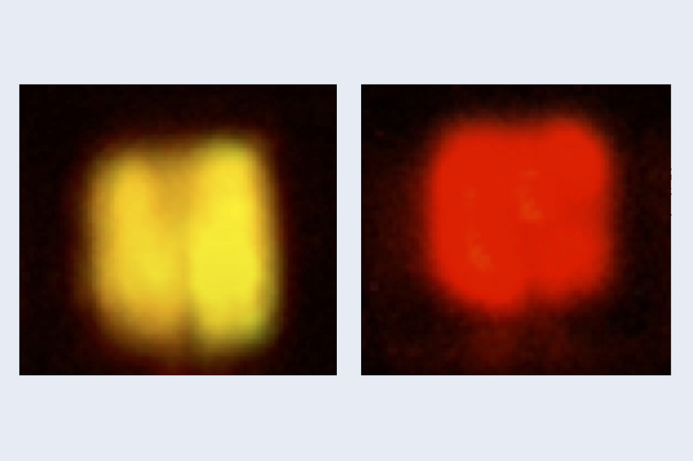
On-wafer measurements revealed a peak at 646 nm, when driving the device at 5 A cm-2. For the control – produced with the same process, but on sapphire – the peak is at 590 nm at the same current density. Pasayat and co-workers attribute the substantial difference in emission wavelength to the more efficient indium incorporation in the quantum wells grown on porous GaN pseudo-substrates.
Driven at 10 A cm-2, EQE of the microLED peaks at 0.202 percent. Encapsulation should increase this figure to more than 0.6 percent. Cranking up the current to 100 A cm-2 propelled light output to 76 nW, corresponding to 2.1 W mm-2 – this output power density just exceeds that of the best AlGaInP microLEDs, which are 20 μm in size.
The team’s next goal is to increase the EQE of its devices. “We are planning on improving the material quality, as well as the fabrication steps,” says Pasayat.
Pictured above: the team at UCSB has produced yellow and red InGaN LEDs. The images are taken for a drive current of 5 A cm-2.


