
Sussex team develops ultra-thin terahertz source
Illuminating ultra-thin layers of InAs with two different types of laser light, produces short bursts of terahertz radiation
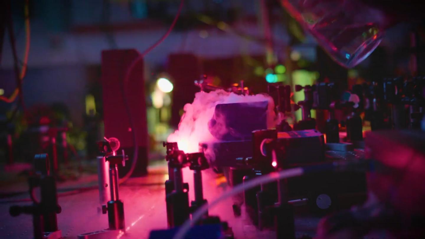
Physicists from the University of Sussex, UK, have developed an extremely thin, large-area semiconductor surface source of terahertz, composed of just a few atomic layers of the narrow bandgap compound semicdonductor InAs.
By illuminating the InAs with red (800nm wavelength) and blue (400nm wavelength) laser light, they were able to elicit the emission of short bursts of Terahertz radiation. The generation depends directly on the relative phase between the two colours.
They published their findings in the journal Physical Review Letters.

The figure above shows the experimental setup. (a) The red, blue, and green beams denote the 800, 400nm, and THz beam paths, respectively. The inset displays the role played by the phase delay. (b) A schematic of the whole setup. Half-wave plate (HWP), barium borate crystal (BBO), Calcite plate (CP), fused silica window (SW: UV), Quarter-wave plate (QWP), ZnTe.
Terahertz sources emit brief light pulses oscillating at 'trillion of times per second'. At this scale, they are too fast to be handled by standard electronics, and, until recently, too slow to be handled by optical technologies. This has great significance for the evolution of ultra-fast communication devices above the 300GHz limit - such as that required for 6G mobile phone technology - something that is still fundamentally beyond the limit of current electronics.
Researchers in the Emergent Photonics (EPic) Lab at Sussex, led by Marco Peccianti, have achieved the brightest and thinnest surface semiconductor sources demonstrated so far. The emission region of their new development, a semiconductor source of terahertz, is ten times thinner than previously achieved, with comparable or even better performances.
The thin layers can be placed on top of existing objects and devices, meaning they are able to place a terahertz source in places that would have been inconceivable otherwise, including everyday object such as a teapot or even a work of art - opening up huge potential for anti-counterfeiting and 'the internet of things' - as well as previously incompatible electronics, such as a next generation mobile phone.
Juan S. Totero Gongora, Leverhulme Early Career Fellow at the University of Sussex, said: "From a physics perspective, our results provide a long-sought answer that dates back to the first demonstration of terahertz sources based on two-colour lasers Our findings therefore open up a wide range of exciting opportunities for terahertz technologies."
Luke Peters, research fellow of the European Research Council project TIMING at the University of Sussex, said: "The idea of placing terahertz sources in inaccessible places has great scientific appeal but in practice is very challenging. Terahertz radiation can have a superlative role in material science, life science and security. Nevertheless, it is still alien to most of the existing technology, including devices that talk to everyday objects as part of the rapidly expanding 'internet of things'.
" This result is a milestone in our route to bring terahertz functions closer to our everyday lives."
Previous developments from Peccianti's team showcased the potential applications of terahertz cameras, which could be transformative in airport security, and medical scanners - such as those used to detect skin cancers.
One of the biggest challenges faced by scientists working in terahertz technology is that what is commonly accepted as an 'intense terahertz source' is faint and bulky when compared with, for example, a light bulb. In many cases, the need for very exotic materials, such as nonlinear crystals, makes them unwieldy and expensive. This requirement poses logistical challenges for integration with other technologies, such as sensors and ultrafast communications.
The research was developed within the framework of the European Research Council project "TIMING".
'All-Optical Two-Color Terahertz Emission from Quasi-2D Nonlinear Surfaces' by J. S. Totero Gongora et al; Phys. Rev. Lett. 21 December 2020


