
GaN HEMTs deliver record efficiency
Native, treated substrates enable GaN HEMTs to surpass 80 percent power-added efficiency
Engineers from Fujitsu are claiming to have raised the bar for the power-added efficiency (PAE) of GaN HEMTs operating at a few gigahertz. Their record-breaking device delivers a PAE of nearly 83 percent when operating at 2.45 GHz.
This high efficiency could help to drive down the carbon footprint of wireless infrastructure. According to findings from a project entitled Energy Aware Radio and Network Technologies, power amplifiers typically account for 65 percent of the energy consumption of a radio base station.
The team from Fujitsu fabricated its devices on free-standing GaN substrates, a foundation that spokesman Yusuke Kumazaki describes as “affordable”. However, he admits that it’s still expensive compared with other common substrates, and the price must come down to ensure commercial success of GaN-on-GaN devices.
Producing GaN HEMTs on native substrates slashes the defect density in the epilayers, leading to suppression of current collapse, a cause of degradation of power characteristics. However, prior to this latest work from Fujitsu, GaN-on-GaN HEMTs have failed to deliver the anticipated superior RF performance to siblings produced on other substrates. Kumazaki and co-workers suspected that silicon contamination at the interface was to blame for holding back the RF performance. “But the impact of silicon contamination on RF performance is much greater than our assumption,” admits Kumazaki.
Note that when GaN HEMTs are grown on foreign substrates, such as silicon or SiC, silicon contamination at the growth interface is not a significant issue. That’s because these epistructures feature wider bandgap materials, such as the AlN nucleation layer, where silicon does not act as a donor.
To suppress silicon impurity contamination, Fujitsu’s engineers treat substrates with hydrofluoric acid before growing the epilayers. The superiority of this approach has been proven by comparing material characteristics and HEMT performance of structures produced with and without the hydrofluoric acid, wet-chemical treatment.
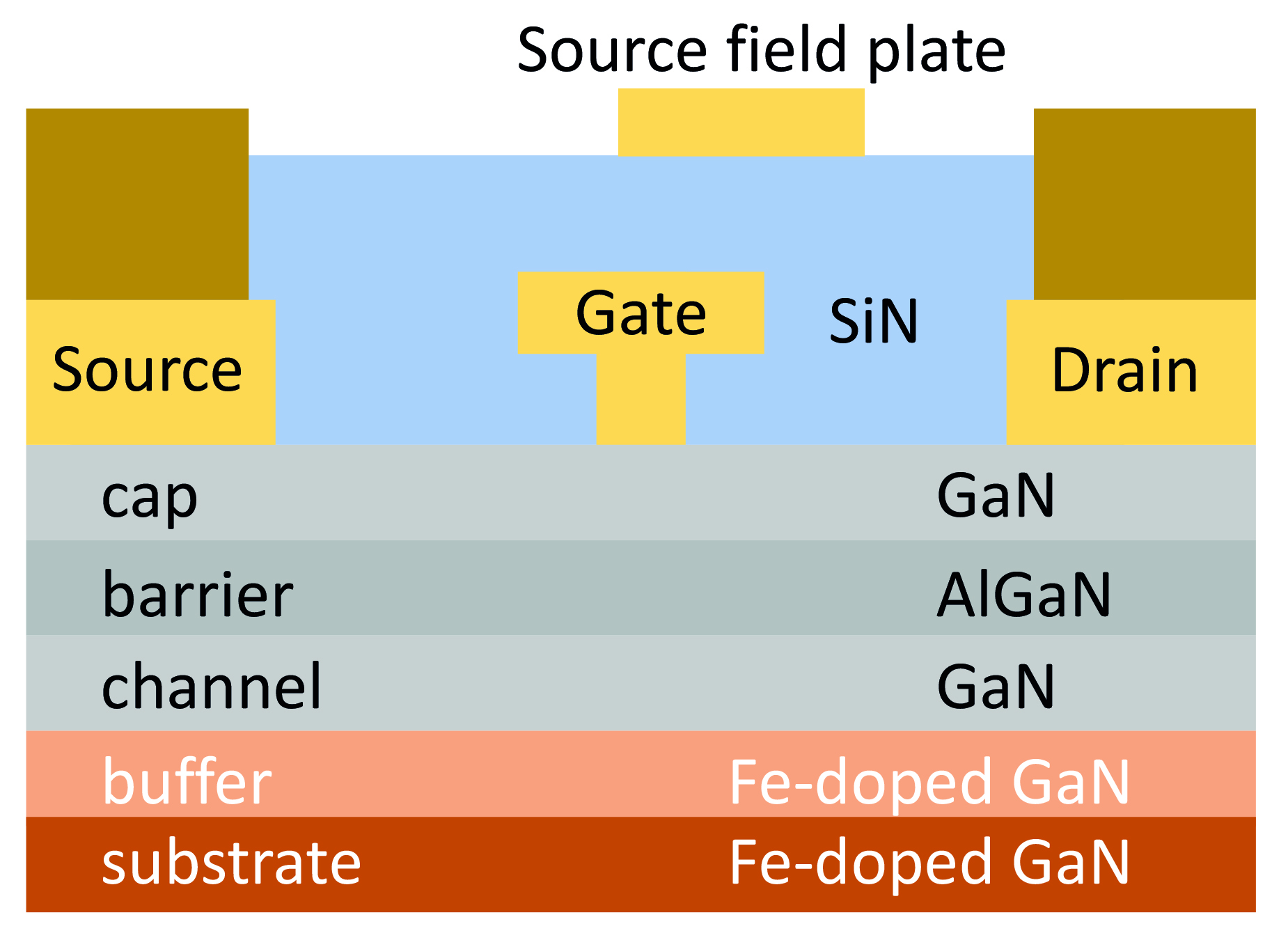
Devices for this study were grown by MOCVD. They featured surface passivation and a source-connected field plate, to reduce the electric field at the gate edge (see Figure 1 above).
Secondary-ion mass spectrometry revealed that silicon piles up at the interface between the substrate and the epilayers in GaN HEMT produced with both processes, despite the lack of intentional silicon doping. However, silicon accumulation in the control peaks at 5 x 1019 cm-3, compared with just 8 x 1017 cm-3 in the HEMT produced with a hydrofluoric acid treatment.

Figure 2. By preventing silicon contamination at the epilayer-substrate interface, Fujitsu’s GaN HEMTs are setting a new benchmark for power-added efficiency at 2.45 GHz, which is within the industrial, scientific and medical band.
'Over 80% power-added-efficiency GaN high-electron-mobility transistors on free-standing GaN substrates' by Y. Kumazaki et al. Appl. Phys. Express 14 016502 (2021)


