
Ultraviolet LEDs get smaller and brighter
Arrays of miniaturised deep-UV LEDs deliver record brightness
Scientists at the University of South Carolina are claiming to have produced the world’s smallest and brightest deep-UV LEDs. Their devies, emitting at 281 nm, have dimensions down to 5 μm, with arrays producing an output of up to 361 W cm-2.
The team’s progress will help this class of LED compete against mercury lamps in applications requiring high doses of deep-UV radiation. For some applications, such as face-mask disinfection, the toxicity of mercury is of concern.
Led by Asif Khan, the team at the University of South Carolina pioneered interconnected arrays of tiny UV LEDs in the early years of this millennium. Introduced to combat series resistance and aid current spreading, the first generation of UV LED pixels with a 25 μm diameter provided the building blocks for 10 by 10 arrays that combined an increase in light output power with superior device reliability and reduced current crowding.
Recently, the team revisited this architecture for a deep UV source, focusing this investigation on thermal impedance and the influence of pixel size on the power of the emission.
Spokesman for the latest work, Richard Floyd, told Compound Semiconductor that reducing the dimensions of the deep UV LEDs below 20 μm did not increase the difficulty of most fabrication steps, and did not require specialised equipment. “For instance, we used standard photoresist masking and a Karl Suss MJB-3 mask aligner for all the lithography steps.”
However, to ensure good uniformity across the wafer, the team optimised the photolithography exposure/developing times for sub-20 μm features, and the p-ohmic contact annealing condition.
The engineers are confident that even smaller deep-UV LEDs could be produced without compromising performance. “In our study we noted that the external quantum efficiency of the interconnected micropixel arrays did not reduce with reducing pixel size,” remarks Floyd. “This implies that pixel sizes smaller than those of our study may be realized without sacrificing device performance.”
Note, however, that the team’s results indicate that there will only be a minimal reduction in thermal impedance from further shrinking of device size.
Fabrication of the UV sources began by loading AlN-on-sapphire templates into an MOCVD chamber and depositing an epistructure that includes four 2.5 nm-thick Al0.35Ga0.65N quantum wells and a 20 nm-thick p-type Al0.7Ga0.3N electron-blocking layer. Inductively couple plasma reactive-ion etching defined pixel dimensions, before annealing under nitrogen activated the magnesium dopants and ‘narrow picture frame’ n-contacts were added, around single pixels in standalone devices and around the subarrays of pixels in interconnected devices. According to previous studies, this n-contact geometry precludes current crowding.
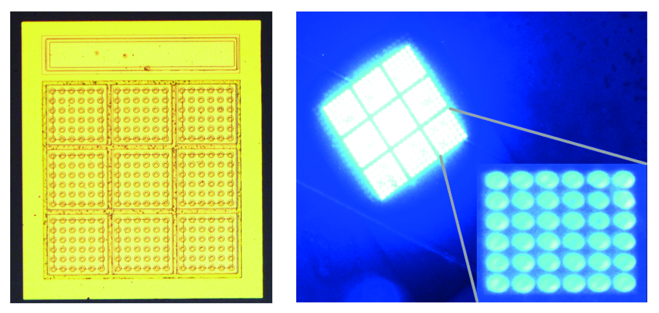
Floyd and colleagues compared the performance of a reference single-pixel LED that has a diameter of 90 μm with three different array architectures: 36 pixels with a 15 μm diameter and a 5 μm gap, 81 pixels with a 10 μm diameter and a 5 μm gap, and 324 pixels with a 5 μm diameter and a 5 μm gap.
On-wafer measurements – using 500 ns pulses and a 0.05 percent duty cycle to minimise device heating – revealed that for a single 5 μm-diameter pixel with an aluminium heat spreader, a drive current of 10.2 kA cm-2 led to a peak brightness of 291 W cm-2. This brightness is 30 times higher than that of the reference LED.
Results from the three different arrays show that reducing the pixel size boosts performance, thanks to superior heat extraction that quashes thermal droop. Compared with the single-chip reference, the array of 324 pixels with a diameter of 5 μm delivered an increase in the output power of more than five times under CW operation, and more than 15 in pulsed mode.
The picture at the top of the article shows (left) top-side micrograph of an interconnected array of 5 μm pixels with 5 μm interpixel spacing, and (right) sapphire-side micrograph of the same array under a 60 mA DC current.
The team are now exploring techniques for enhancing light extraction efficiency, and looking to leverage independent electronic control of the pixels.
R. Floyd et al. Appl. Phys. Express 14 014002 (2021)


