
SMART Breakthrough Enables Twistronics
Stacking films at a twist angle allows a new way to control light emitting from materials
Researchers from the Low Energy Electronic Systems (LEES) Interdisciplinary Research Group (IRG) at Singapore-MIT Alliance for Research and Technology (SMART), MIT’s research enterprise in Singapore together with Massachusetts Institute of Technology (MIT) and National University of Singapore (NUS) have discovered a new way to control light emission from materials.
Controlling the properties of materials has been the driving force behind most modern technologies – from solar panels, computers, smart vehicles or life-saving hospital equipment. But materials properties have traditionally been adjusted based on their composition, structure, and sometimes size, and most practical devices that produce or generate light use layers of materials of different compositions that can often be difficult to grow.
The breakthrough by SMART researchers and their collaborators offers a new approach to tune the optical properties of technologically-relevant materials by changing the twist angle between stacked films, at room temperature. Their findings could have an impact on various applications in the medical, biological, and quantum information fields. The team explain their research in a paper titled 'Tunable Optical Properties of Thin Films Controlled by the Interface Twist Angle' recently published in Nano Letters.
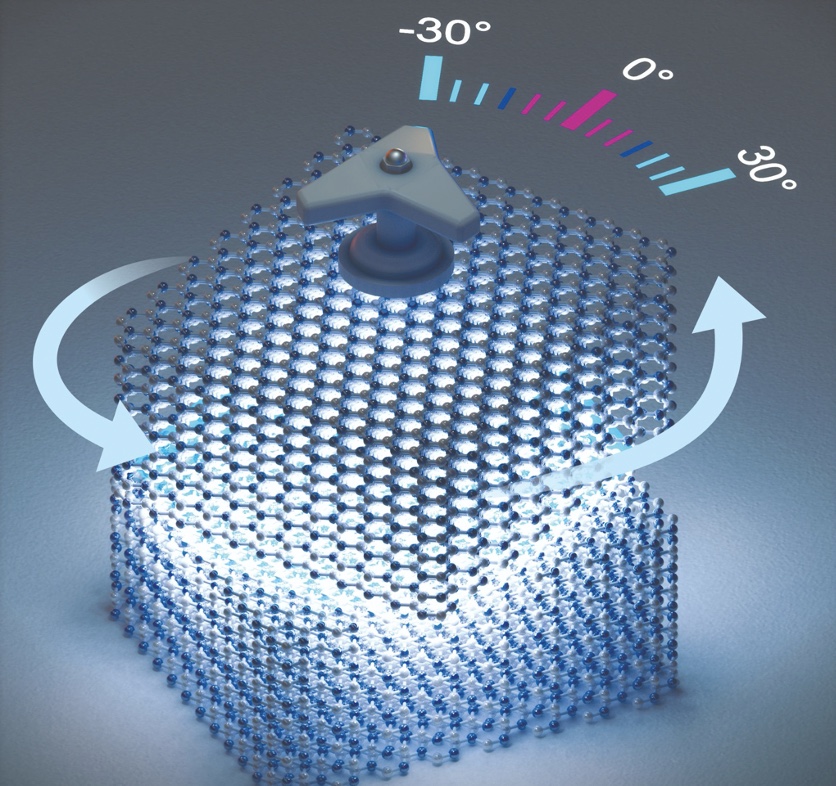
“A number of new physical phenomena – such as unconventional superconductivity – have been discovered recently by stacking individual layers of atomically-thin materials on top of each other at a twist angle, which results in the formation of what we call moiré superlattices,” says corresponding author of the paper, Silvija Gradecak from the Department of Materials Science and Engineering at NUS and Principal Investigator at SMART LEES. “The existing methods focus on stacking only thin individual monolayers of film which is laborious, while our discovery would be applicable to thick films as well – making the process of materials discovery much more efficient.”
Their research can also be meaningful for developing the fundamental physics in the field of 'twistronics' – the study of how the angle between layers of two-dimensional materials can change their electrical properties. Professor Gradecak points out the field has so far focused on stacking individual monolayers, which requires careful exfoliation and may suffer from relaxation from a twisted state, thus limiting their practical applications. The team’s discovery could make this groundbreaking twist-related phenomenon applicable to thick film systems as well, which are easy to manipulate and industrially relevant.
“Our experiments showed that the same phenomena leading to formation of moiré superlattices in two-dimensional systems can be translated to tune optical properties of three-dimensional, bulk-like hexagonal boron nitride (hBN) even at room temperature,” said Hae Yeon Lee, the lead author of the paper and a Materials Science and Engineering PhD candidate at MIT. “We found that both the intensity and colour of stacked, thick hBN films can be continuously tuned by their relative twist angles and intensity increased by more than 40 times.”
The research results open up a new way to control optical properties of thin films beyond the conventionally used structures especially for applications in medicine, environmental or information technologies.
The research is carried out by SMART and supported by the National Research Foundation (NRF) Singapore under its Campus for Research Excellence And Technological Enterprise (CREATE) programme.


