
A new way to find GaN imperfections
Osaka University team reports nondestructive method for identifying threading dislocations in GaN substrates
Researchers at Osaka University have reported a nondestructive method for characterising the crystalline quality of GaN. Their findings were published in Applied Physics Express.
GaN power switching devices offer numerous advantages including high-speed switching, high-power operation, low on-resistance, and high breakdown voltage. To take advantage of these properties, the defect density of GaN crystals must be low.
Threading dislocations (TDs) are a type of crystal defect generated by the imperfection of crystals that propagate from the substrate into an epitaxial layer. These TDs often serve as leakage current paths.
TDs can be classified using their Burgers vectors. A variety of methods can be used to analyse GaN and determine the Burgers vectors of the TDs; however, most have associated limitations, such as involved sample preparation or limited analysis area. The techniques may also require destructive sample preparation, so tested samples cannot be reused.
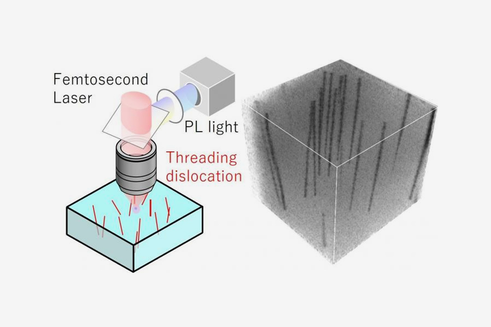
The researchers therefore used multiphoton excitation photoluminescence (MPPL) to evaluate GaN. MPPL is a nondestructive technique in which the excitation laser light penetrates deep into the samples. It is therefore ideal for the three-dimensional (3D) evaluation of crystal defects in materials.
"We used MPPL to carry out an in-depth study of defects in GaN crystals by analyzing the local photoluminescence properties and the 3D defect structures," explains study first author Mayuko Tsukakoshi. "Considering our findings along with those of the etch pit method then allowed for statistical classification of the TDs."
"Being able to relate MPPL findings to the quality of GaN crystals provides an excellent tool for nondestructive, high throughput substrate evaluation," study corresponding author Tomoyuki Tanikawa says. "We believe our findings will help to easily identify defects that affect reliability, as well as improve yields to give more efficient routes to GaN devices."

Picture above: From the contrast difference of the dark line and the distribution map of the inclination angle from the c-axis (left), it can be seen that the TDs have three types of properties. From the inclination angle and the distribution in the in-plane direction of the inclination (right), the distribution has a six-fold symmetry according to the in-plane symmetry of the Burgers vector of mixed TDs. The mixed TDs were found to extend through GaN at large inclination angles. In addition, the contrast of the photoluminescence signals indicated that the screw TDs had stronger nonradiative properties than the others.
'Identification of Burgers vectors of threading dislocations in free-standing GaN substrates via multiphoton-excitation photoluminescence mapping' by Mayuko Tsukakoshi et al; Applied Physics Express, Volume 14, Number 5 (2021)


