Loading...
News Article

K-Space releases new Spectral Reflectance Product

News

Non-contact metrology solution uses method developed at Sandia National Laboratory

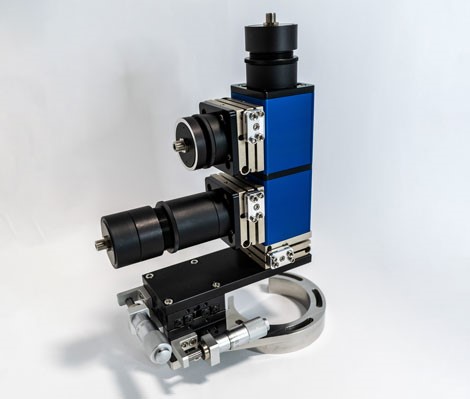
k-Space Associates ans released the kSA SpectR, a complete non-contact metrology solution for measuring absolute spectral reflectance, L*a*b* colour parameters, and growth rate.

This tool has many applications for in situ monitoring and process control, including VCSELs, distributed Bragg reflectors (DBRs), and other complex device structures. Thin-film production and research facilities can use it in sputtering, MBE, and MOCVD growth methods.

The kSA SpectR optics are configured in a specular reflectance geometry. k-Space uses a method that was developed at Sandia National Laboratory and is licensed to k-Space. In this approach, the fitting routine restarts with each new layer, treating the underlying film stack as a 'virtual' substrate.

The kSA SpectR can perform measurements simultaneously at multiple wavelengths, each of which offers potential advantages. This tool easily measures custom spectral features such as reflectance minima, maxima, inflection points, or baseline scatter level, over a user-defined wavelength range of interest.

Darryl Barlett, CEO of k-Space, said: “This tool, like many of our tools, is the direct result of a specific customer need. When the customer came to us, we listened to their measurement requirements and then designed a system, incorporating Sandia National Laboratory’s technology, that worked for their application.

"As the complexity of thin-film layers advances, so does the need for metrology that measures the right parameters for yield and performance. This system has the capability to work on complex thin-film structures, including applications such as precisely determining the Fabry-Perot dip during DBR growth.”

SiC MOSFETs: Understanding the benefits of plasma nitridation
Wolfspeed reports Q2 results
VueReal secures $40.5m to scale MicroSolid printing
Mitsubishi joins Horizon Europe's FLAGCHIP project
Vishay launches new high voltage SiC diodes
UK team leads diamond-FET breakthrough
GaN adoption at tipping point, says Infineon
BluGlass files tuneable GaN laser patents
QD company Quantum Science expands into new facility
Innoscience files lawsuit against Infineon
Riber revenues up 5% to €41.2m
Forvia Hella to use CoolSiC for next generation charging
Photon Design to exhibit QD simulation tool
Ortel transfers CW laser fabrication to Canada
Luminus adds red and blue multi-mode Lasers
PseudolithIC raises $6M for heterogeneous chiplet tech
Mesa sidewall design improves HV DUV LEDs
IQE revenue to exceed expectations
'Game-changing' VCSEL system targets clinical imaging
German start-up secures finance for SiC processing tech
Macom signs preliminaries for CHIPS Act funding
IQE and Quintessent partner on QD lasers for AI
EU funds perovskite tandems for fuel-free space propulsion
EU to invest €3m in GeSi quantum project
Transforming the current density of AlN Schottky barrier diodes
Turbocharging the GaN MOSFET with a HfO₂ gate
Wolfspeed launches Gen 4 SiC MOSFET technology
Report predicts high growth for UK's North East
Element Six unveils Cu-diamond composite
SemiQ launches hi-rel 1700V SiC MOSFETs
Lynred to exhibit Eyesential SWIR sensor for machine vision
Thorlabs buys VCSEL firm Praevium Research
×
Search the news archive

To close this popup you can press escape or click the close icon.
Logo
x
Logo
×
Register - Step 1

You may choose to subscribe to the Compound Semiconductor Magazine, the Compound Semiconductor Newsletter, or both. You may also request additional information if required, before submitting your application.


Please subscribe me to:


You chose the industry type of "Other"

Please enter the industry that you work in: