
German consortium to develop hack-proof comms solution
€15 million Silhouette project to produce 'made in Europe' electro-optic quantum cryptography platform
Connected devices are making their way into more and more areas of everyday life. However, these are often vulnerable to cyberattacks. A German consortium of industry, university and research institutes aims to make these systems more secure in the future thanks to light-based data transmission and computation.
Over the next three years, the Silhouette project (Silicon Photonics for Trusted Electronic Systems) will develop universally applicable solutions. The German Federal Ministry for Education and Research BMBF is funding the €15 million project to the tune of €12 million.
The consortium is made up of the Fraunhofer Institute for Photonic Microsystems IPMS from Dresden as project coordinator, the Fraunhofer Institute for Reliability and Microintegration IZM from Berlin with its institute branch IZM-ASSID in Moritzburg, the Fraunhofer Institute for Telecommunications HHI from Berlin, the Institute of Electronic Packaging Technology (IAVT) and the Integrated Photonic Devices (IPD) group of the Technical University of Dresden. The technology developer and manufacturer is Osram Opto Semiconductors from Regensburg, and the quantum optics developer and marketer qutools from Munich. The project runs from 2021 to 2024.
By 2025, an increase from 30 to 75 billion IoT devices is forecast. Accordingly, global efforts are underway to improve the security of these assets to protect sensitive data from misuse by third parties. Strong, hardware-supported cryptographic algorithms are one of the methods being used to achieve this.
However, with increasing communication speeds, the negative cost and energy budget grows. “By expanding silicon-based technologies to include photonic, i.e. light-based, special components, we can address this issue,” explains Marcus Pietzsch, a scientist at the Fraunhofer Institute for Photonic Microsystems IPMS in Dresden and coordinator of the Silhouette project.
The project aims to create a universal platform solution for developing such hybrid systems. The key point is to convert safety-critical electrical signals into optical signals, further process or validate them and finally convert them back. “Photonic transmission channels alone offer the advantage of being both virtually impossible to manipulate and tap-proof,” Pietzsch continues.
The hybrid approach of the consortium allows the use of existing safety-critical components from third-party suppliers, so that the current range of applications can ideally be maintained. The project covers the entire value chain: from the design of the electrical and optical components, through manufacturing, assembly and interconnection technology, to testing and inspection.
Particular attention is being paid to ensure short time-to-market. "At present, it is still difficult to produce hybrid electro-optical circuits cost-effectively and in large quantities," says Pietzsch. Therefore, the project partners will pool their expertise to develop prototypes which already contain features of secure products suitable for mass production.
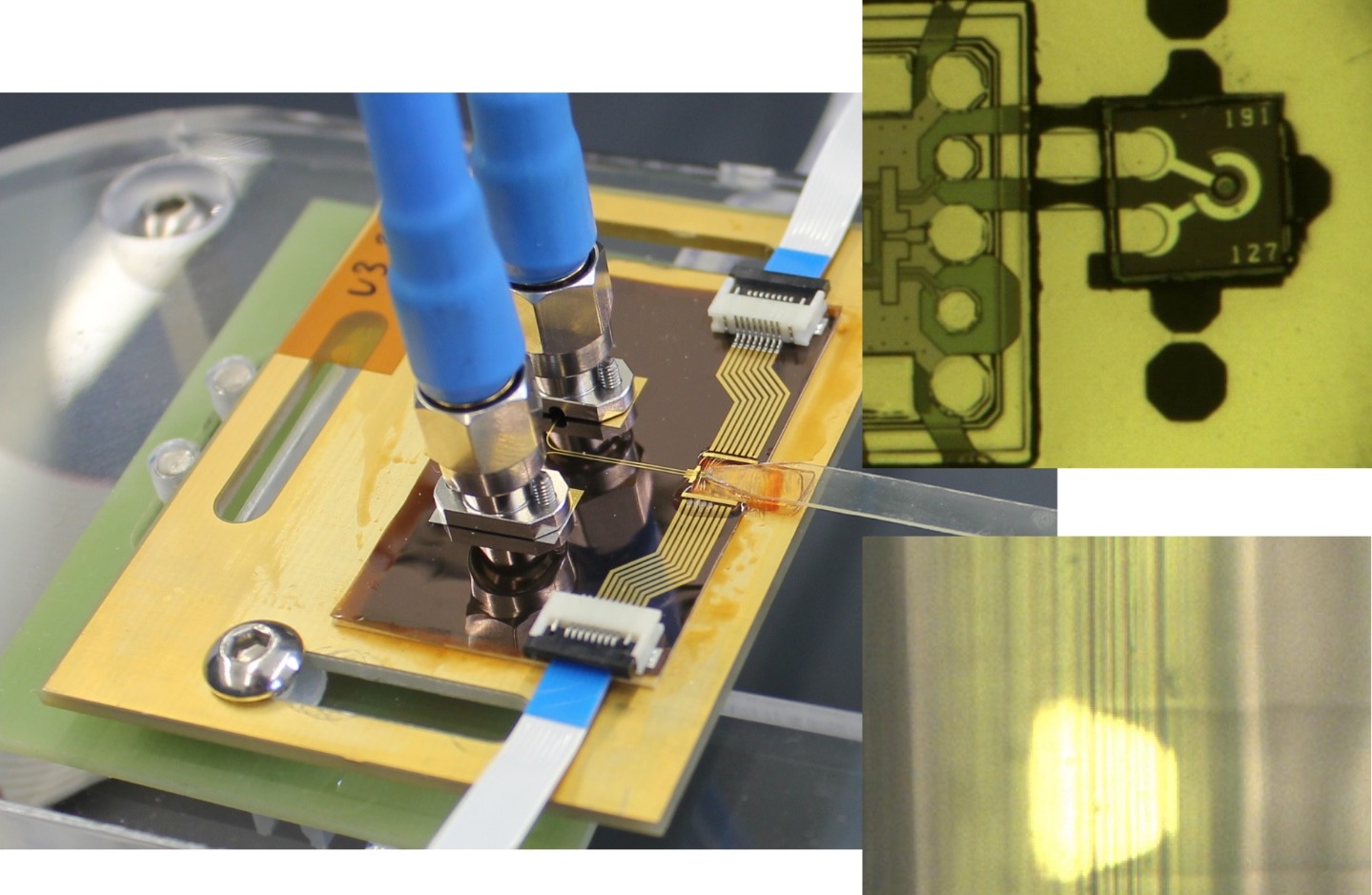
The picture at the top of the page shows a demonstration of optical data transmission via polymer planar optical fibres. Top right: Direct metal contacts between additive embedded VCSEL and laser driver. Bottom right: Integration of 45 degree micromirrors into polymer optical fibers.
'Made in Europe' platform
The desired electro-optical (E/O) platform solution is 'made in Europe' in order to be able to guarantee technological sovereignty and trustworthiness also in the design and manufacturing process. In contrast to microelectronics, Germany can demonstrate a development lead in photonics across the board. “In order to maintain this lead and, in perspective, achieve sovereignty in manufacturing, photonic components must be more accessible. The prerequisite for this is the simplest possible universal interface to existing digital components, which will continue to be indispensable,” says Pietzsch.
The largest market segment for photonic components currently is the telecommunications sector. The photonic security technologies developed in project “Silhouette” are therefore geared to the specific security requirements of this market segment. “Subject areas beyond this, such as AI, simulation and complex mathematical optimisation problems, are either still in the development or prototype stage or are being manufactured as small series with low volumes,” explains Pietzsch. “The consortium sees great potential here to make these technologies accessible to a broad user group and at the same time to open up completely new fields of application.”


