
Smallest acoustic amplifier emerges from 50-year-old hypothesis
Sandia National Lab's acoustoelectric device reveals new road to miniaturising wireless tech
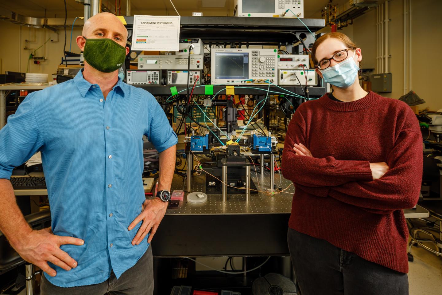
Scientists at Sandia National Laboratories in the US have built what they believe is the world's smallest and best acoustic amplifier. And they did it using a concept that was all but abandoned for almost 50 years.
As detailed in the paper published May 13 in Nature Communications, the device is more than ten times more effective than the earlier versions. The design and future research directions hold promise for smaller wireless technology.
"Acoustic wave devices are inherently compact because the wavelengths of sound at these frequencies are so small - smaller than the diameter of human hair," Sandia scientist Lisa Hackett said. But until now, using sound waves has been impossible for many of these components.
Sandia's acoustic, 276-megahertz amplifier, measuring 0.5 square millimeters, demonstrates the vast, largely untapped potential for making radios smaller through acoustics. To amplify 2 GHz frequencies, which carry much of modern cell phone traffic, the device would be even smaller, 0.02 square millimeter, a footprint that would comfortably fit inside a grain of table salt and is more than ten times smaller than current state-of-the-art technologies.

Their heterogeneously integrated acoustoelectric material platform consists of a 50 nm InGaAs epitaxial semiconductor film in direct contact with a 41° YX lithium niobate piezoelectric substrate. Using this approach, they demonstrated three of the main components of an all-acoustic RF signal processor: passive delay line filters, amplifiers, and circulators.
According to the team, heterogeneous integration allows for simultaneous, independent optimisation of the piezoelectric-acoustic and electronic properties, leading to the highest performing surface acoustic wave amplifiers ever developed in terms of gain per unit length and DC power dissipation, as well as the first-ever demonstrated acoustoelectric circulator with an isolation of 46 dB with a pulsed DC bias.
Sandia scientist Matt Eichenfield said: "We are the first to show that it's practical to make the functions that are normally being done in the electronic domain in the acoustic domain."
Resurrecting a decades-old design
Scientists tried making acoustic RF amplifiers decades ago, but the last major academic papers from these efforts were published in the 1970s.
Without modern nanofabrication technologies, their devices performed too poorly to be useful. Boosting a signal by a factor of 100 with the old devices required 1cm of space and 2,000 V. They also generated lots of heat, requiring more than 500 milliwatts of power.
The new and improved amplifier is more than 10 times as effective as the versions built in the '70s in a few ways. It can boost signal strength by a factor of 100 in 0.2mm with only 36 volts of electricity and 20 milliwatts of power.
Previous researchers hit a dead end trying to enhance acoustic devices, which are not capable of amplification or circulation on their own, by using layers of semiconductor materials. For their concept to work well, the added material must be very thin and very high quality, but scientists only had techniques to make one or the other.
Decades later, Sandia developed techniques to do both in order to improve photovoltaic cells by adding a series of thin layers of semiconducting materials. The Sandia scientist leading that effort happened to share an office with Eichenfield.
"I had some pretty heavy peripheral exposure. I heard about it all the time in my office," Eichenfield said. "So fast forward probably three years later, I was reading these papers out of curiosity about this acousto-electric amplifier work and reading about what they tried to do, and I realised that this work that Sandia had done to develop these techniques for essentially taking very, very thin semiconductors and transferring them onto other materials was exactly what we would need to make these devices realise all their promise."
Fusing the ultrathin InGaAs layer onto the dissimilar acoustic device took an intricate process of growing crystals on top of other crystals, bonding them to yet other crystals and then chemically removing 99.99 percnent of the materials to produce a perfectly smooth contact surface. Nanofabrication methods like this are a research area of growing interest at Sandia's Microsystems Engineering, Science and Applications complex.
Work was funded by Sandia's Laboratory Directed Research and Development program and the Center for Integrated Nanotechnologies, a user facility jointly operated by Sandia and Los Alamos national laboratories.
According to Eichenfield, converting mass-produced, commercial products like cell phones to all acousto-electric technology would require a massive overhaul of the manufacturing infrastructure. But for small productions of specialised devices, the technology holds more immediate promise.
The Sandia team is now exploring whether they can adapt their technology to improve all-optical signal processing, too. They are also interested in finding out if the technology can help isolate and manipulate single quanta of sound, called phonons, which would potentially make it useful for controlling and making measurements in some quantum computers.
'Towards single-chip radiofrequency signal processing via acoustoelectric electron–phonon interactions' by Lisa Hackett et al; Nature Communications volume 12, (2021)


