
Innovative Co-Packaged Optics Chip for Hyperscale Data centres
Ranovus extends partnership with IBM, TE Connectivity, and Senko Advanced Components to deliver significant power and cost savings with CPO 2.0 technology
At the optical networking event OFC 2021 in San Francisco this week, Ranovus has revealed the next step in reducing power consumption and overall costs for hyperscale data centre operations with the introduction of the Odin Analog-Drive CPO 2.0 architecture.
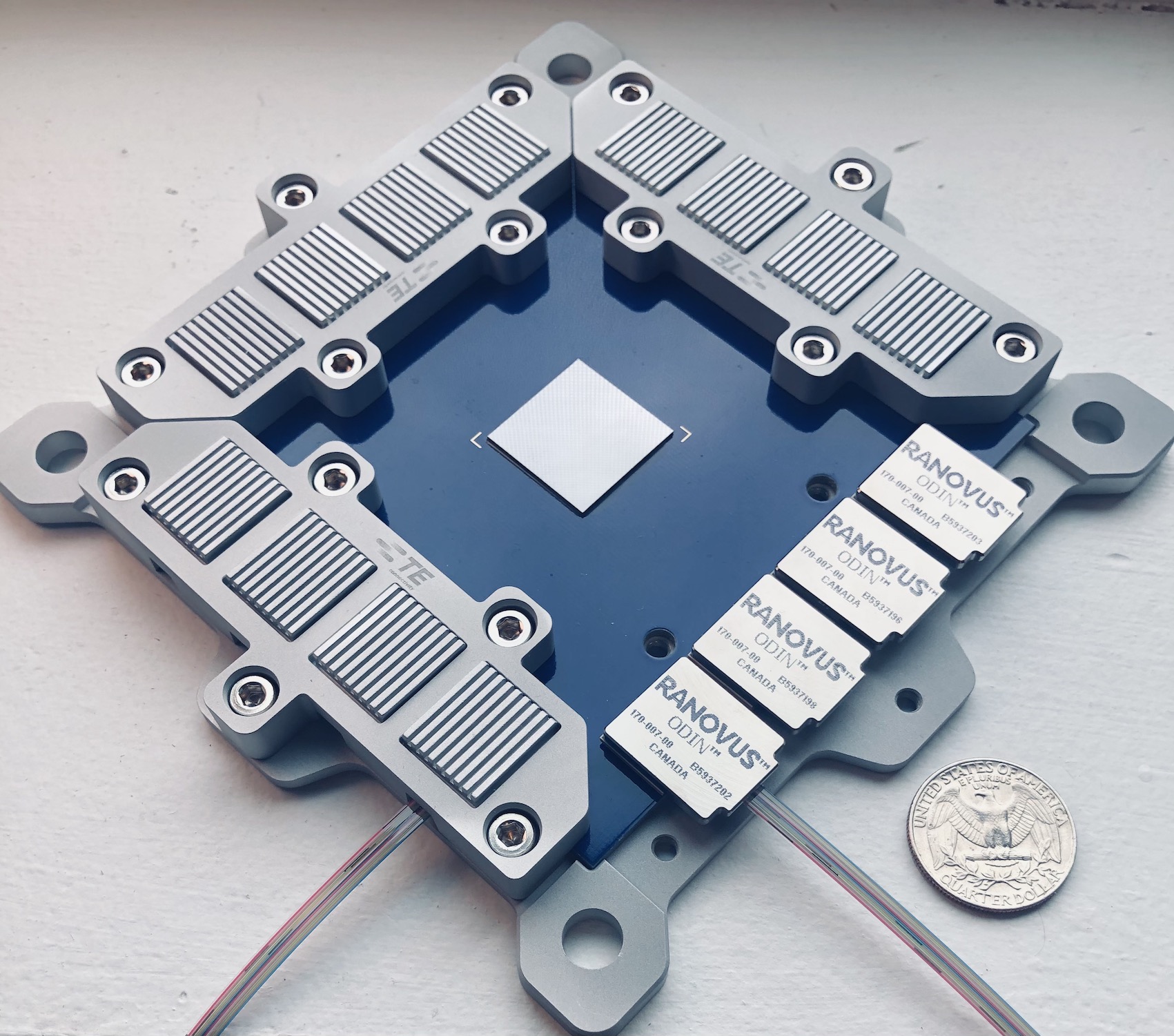
Ranovus has collaborated with providers of multi-terabit interconnect solutions IBM, TE Connectivity, and Senko Advanced Components to create this second- generation CPO 2.0 configuration for the data centre.
Co-packaged Optics, or CPO, is an innovative approach that provides nx100Gbps PAM4 Optical I/O for Ethernet switch and ML/AI silicon in a single packaged assembly, which reduces the cost and power consumption of the complete system.
With data centre traffic growing at an unprecedented pace, fuelled by advances in AI and Machine Learning, the networking infrastructure must scale in capacity while maintaining its total power consumption and footprint. The collaboration announced in March 2020 between Ranovus, TE, IBM, and SENKO, known as CPO 1.0, has enabled an attractive multi-sourced solution to further meet this challenge.
CPO 2.0 improves on CPO 1.0 while maintaining optical interoperability and brings the following advantages: 40 percent cost and power consumption savings through; eliminating the re-timer function in the Odin Analog-Drive optical engine; enabling a cost-effective single die solution with the Odin Analog-Drive optical engine; smaller footprint; and re-use and optimisation of existing 100G PAM4 and PCIe Ser/Des chips vs new investment in an XSR Ser/Des chip for data centre applications.
Customer trials with Odin Analog-Drive CPO 2.0 are planned in Q4 2021.
Combining capabilities
This collaboration combines a number of capabilities. Ranovus brings its scalable Odin silicon photonics engine, announced at OFC 2020. Odin is built around the company's Multi-Wavelength Quantum Dot Laser (MW QDL), 100Gbps Silicon Photonics based Micro Ring Resonator modulators and photodetectors, 100Gbps Driver, 100Gbps TIA and control circuity in a power efficient and cost-effective single die EPIC (Electronic-Photonic Integrated Circuit).
IBM has contributed its fibre V-groove interconnect packaging technology. This is a robust and reliable assembly technique to interface optical fibres to silicon photonics devices. This process makes use of passive alignment techniques and achieves low insertion loss across a wide spectral range in both the O-band and C-band regimes. The solution is scalable in physical channel count and the automated process provides a path to high-volume manufacturing of co-packaged optics.
TE Connectivity’s co-packaged (CP) fine pitch socket interposer technology enables integration of small chipset and optical engine component technologies into high-value co-package assemblies with reworkable and interoperable interfaces. The CP fine pitch socket interposer technology has signal integrity performance capability for 100 Gbps as well as future 200 Gbps applications. The integration of TE’s controlled force mechanical and thermal bridge hardware completes the assembly by providing an innovative solution for thermal management of the switch, serialiser/deserialiser (SerDes), and optics necessary for high reliability and long operating life.
Senko’s fibre optic connectivity solutions for optical coupling, on-board/mid-board, and faceplate support 100Gbps/lane and beyond Co-Packaged Optics equipment designs. These include low profile and precision fibre coupler assemblies, micro sized on-/mid-board connectors, reflow compatible connector assemblies, space saving connector options for faceplate, and blindmate connector solutions for backplane and external laser source modules. These will provide more efficiency, scalability, and flexibility in designs for Co-Packaged Optics equipment.
“We launched Odin, our next generation monolithic EPIC and laser platform for multi terabit Co-Packaged Optics (CPO) applications in data centres, in March 2020. The Odin platform is a low latency, high density, protocol agnostic monolithic optical engine that delivers massive optical interconnect bandwidth with industry-leading cost and power efficiency,” said Christoph Schulien, EVP of R&D and Systems at Ranovus. “The Odin Analog-Drive configuration eliminates the retimers in the CPO 1.0 configuration, which brings about a 40 percent cost and power reduction to the overall system.”
“IBM is enthusiastic to bring to this collaboration more than 45 years history in microelectronics packaging and its deep experience in optical packaging,” said Paul Fortier, senior engineer, IBM business development. “IBM’s optical assembly processes leverage our automated high-volume semiconductor packaging and IBM’s Assembly and Test division provides the co-packaged optics ecosystem with a seamless end to end manufacturing capability.”
“TE is bringing a holistic solution set to the Co-Packaging effort with our electrical interconnect CP socket technology that can enable CPO miniaturisation along with reworkability,” said Nathan Tracy, Technologist, TE Connectivity, “TE’s thermal bridge technology can be a key enabler to the high density packaging and extreme thermal management necessary for co-packaging.”
“Senko is pleased to contribute our product designs, and IPs to enhance the design capability, scalability, and flexibility for the Co-Packaged Optics embedded products,” said Tiger Ninomiya, Senko's technology & innovation manager. “Innovative optical connectivity solutions are key to making Co-Packaged Optics’ solutions a success in the market.”


