
AlN substrates show much promise for GaN HEMTs
Free-standing AlN substrates have the potential to produce record-breaking X-band HEMTs
Engineers at Fujitsu are claiming to have broken new ground for the performance of the RF GaN-based HEMTs operating in the X-band. Their device, made on an AlN substrate, delivers a power density of more than 15 W mm-1, and far higher values could follow with the introduction of field plates and optimisation of device dimensions.
According to the team, the other reports of GaN-based HEMTs on AlN substrates have used AlGaN channels to improve higher-temperature performance. However, with that design alloy scattering in the ternary diminishes electron mobility and holds back performance. To avoid these issues, the team from Fujitsu employs a GaN channel.
Working with an AlN substrate promises to offer the best of both worlds, as this has a higher conductivity than GaN and avoids the lattice mismatch issues of SiC. But AlN substrates are pricey and limited in size.
Spokesman for the team, Shiro Ozaki, told Compound Semiconductor that he hopes that increased use of these devices for ultraviolet laser diodes and LEDs will help to address these issues. He expect that this will ultimately lead to the availability of affordable, 3-inch diameter substrates.
Ozaki and co-workers have produced a range of GaN HEMTs with a 0.25 μm gate length, a 50 μm gate width and a gate-to-drain length of 3 μm. One of these transistors has been produced on a 1-inch diameter AlN substrate with a threading dislocation density below 103 cm-2, and another five variants have been fabricated on SiC: one, like that on AlN, has a channel thickness of 200 nm, to trim the drain-leakage current; and the other four have 1000 nm-thick channels and different AlGaN barrier compositions, to evaluate the impact of carrier density on DC characteristics.
Measurements of the drain current as a function of the drive voltage, which is the difference between the gate-to-source voltage and the threshold voltage, uncovered a leakage current path for HEMTs that have a thick channel. Devices with the thinner, 200 nm-thick channel supressed this leakage. The team also found that the AlGaN buffer with a high aluminium composition, employed in the device grown on the AlN substrate, sharply reduced the pinch-off state and had a lower leakage current than the similar device made on SiC.
Simulations show that the HEMT on the AlN foundation has a high carrier density, despite its aluminium-rich back-barrier. And, according to these calculations, when the channel thickness is reduced, the electric field in this Al0.3Ga0.7N barrier diminishes, supressing electron tunnelling into this layer and quashing the leakage current.
To ensure excellent output power characteristics, HEMTs must produce a high drain current at a high blocking voltage. Measurements of the five devices made on SiC show that gains on one of these fronts are compromised by losses on the other, while the HEMT on AlN provides an unparalleled performance.
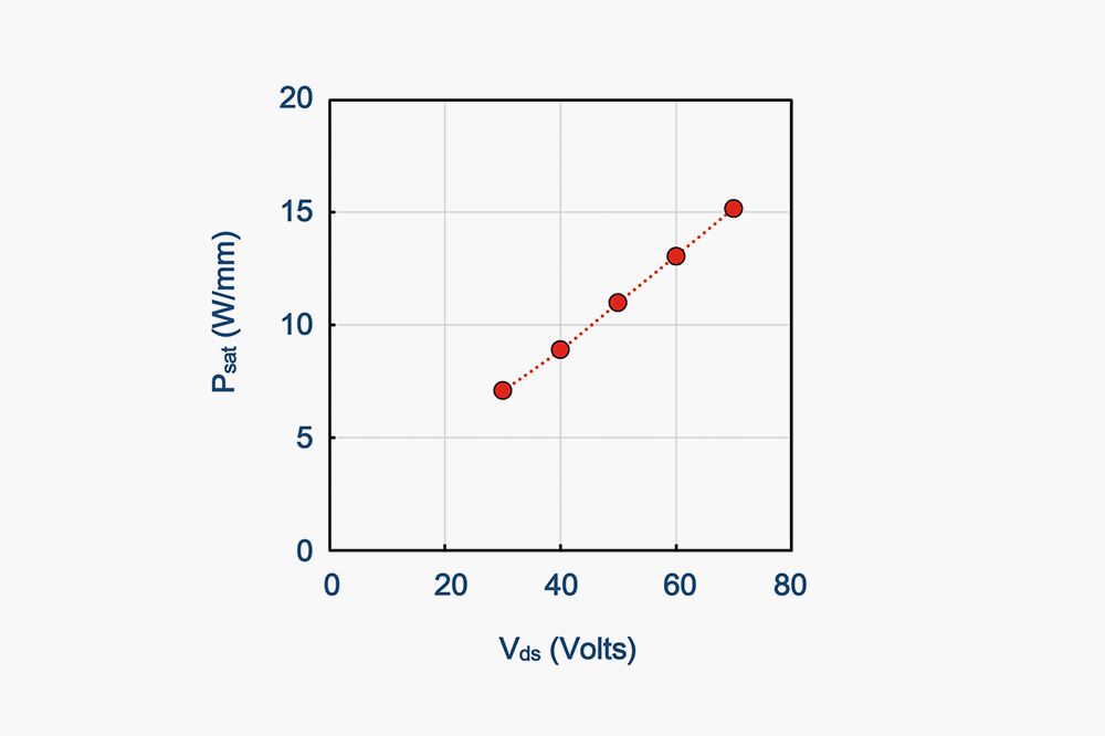
The team’s GaN-on-AlN HEMT, which has a total gate width of 1 mm, produces a peak power-added efficiency of 49.1 percent when operating at 70 V, using 10 μs pulses at a 1 percent duty cycle. Associated output power is 41.7 dB, equivalent to 14.7 W mm-1, and gain is 9.6 dBm.
For devices grown on SiC, a power density of 30.6 W mm-1 has been reported in the X-band. “Our target is higher than that,” says Ozaki.
To meet that goal, Ozaki and co-workers intend to increase the operating voltage for their HEMTs to more than 100 V. “To realise this, field plate optimisation will be a key technology.”
The graph above shows how teh X-band output power of the HEMT made on an AlN substrate increases with operating voltage. Introducing a field plate should enable an increase in the voltage and the output power.
Ozaki et al. Appl. Phys. Express 14 041004 (2021)


