Loading...
News Article

II-VI Introduces Heated Ion Implantation for 150mm SiC Wafers

News

Ion implantation foundry process runs temperatures of up to 650 degC to anneal crystal structure dynamically and eliminate defects.

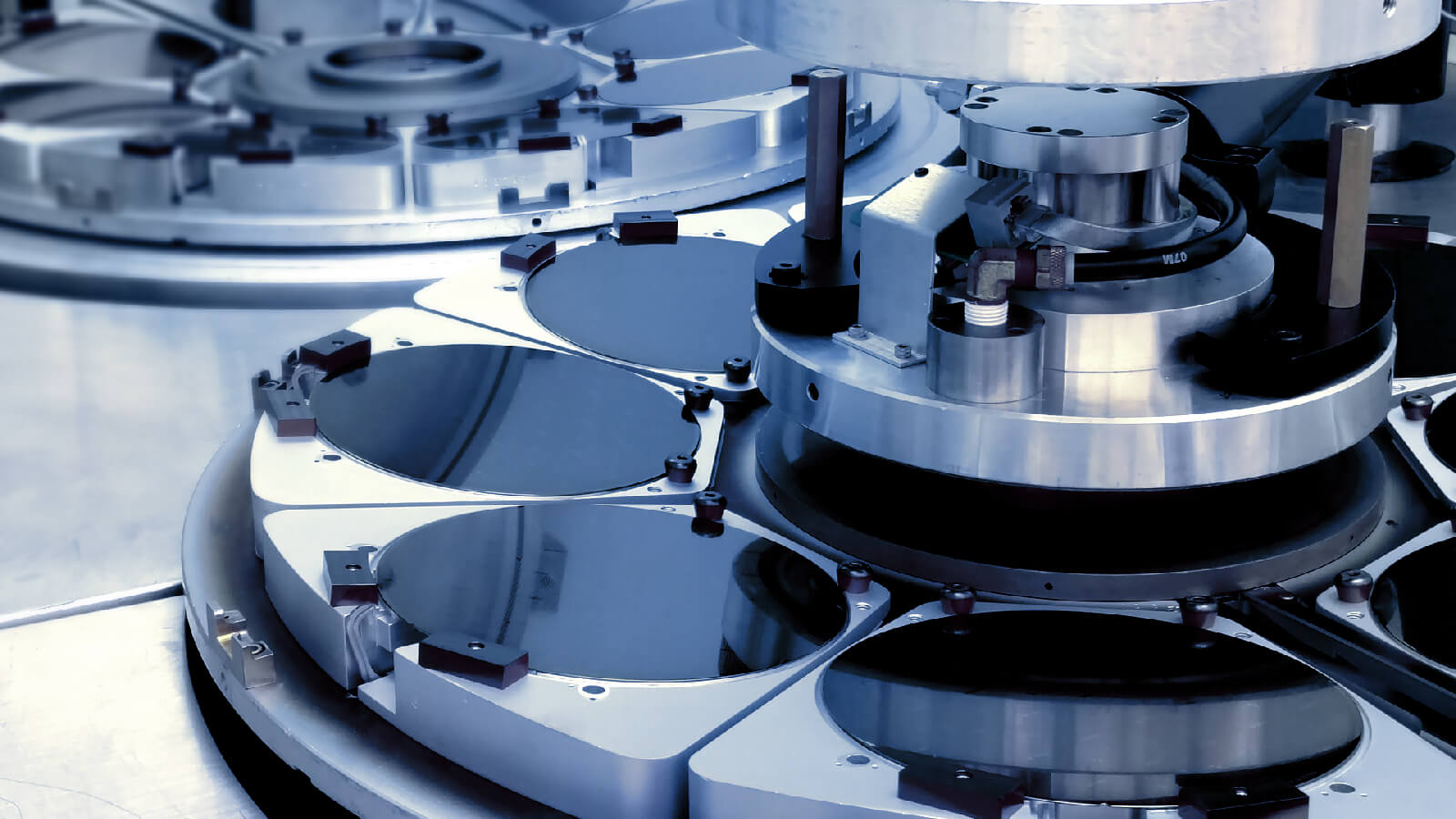
II‐VI, a provider of foundry ion implantation services, has introduced heated ion implantation foundry services for 150 mm SiC wafers.

Acccording to the comany, the process enables highly reliable power electronics by running at temperatures of up to 650degC to anneal the crystal structure dynamically and eliminate defects. The process aldo provides a high level of doping precision, both in terms of depth and concentration.

“To our knowledge, II-VI is the first foundry in the world to provide such advanced ion implantation services commercially for 150 mm SiC wafers and we plan to scale to 200 mm in the future,” said Sohail Khan, executive VP, New Ventures & Wide-Bandgap Electronics Technologies Business Unit.

“II-VI’s new ion implantation process is extremely versatile: It delivers a broad energy range from 10 keV to 1 MeV and can be heated or unheated for a wide range of compound semiconductor wafer materials and devices. This process is compatible with a vast array of materials, including silicon and diamond for special-purpose applications, as well as those that can be integrated into wafer-scale optics platforms.”

II-VI maintains a large complement of high- and medium-current and high-energy production implanters handling 2-inch to 12-inch substrates. II-VI’s broad range of wafer foundry services includes SiC, GaAs, and InP epitaxial growth. II-VI also provides ion implantation disk refurbishing and reconditioning services to maximise quality, uptime, and utilisation.

SiC MOSFETs: Understanding the benefits of plasma nitridation
Wolfspeed reports Q2 results
VueReal secures $40.5m to scale MicroSolid printing
Mitsubishi joins Horizon Europe's FLAGCHIP project
Vishay launches new high voltage SiC diodes
UK team leads diamond-FET breakthrough
GaN adoption at tipping point, says Infineon
BluGlass files tuneable GaN laser patents
QD company Quantum Science expands into new facility
Innoscience files lawsuit against Infineon
Riber revenues up 5% to €41.2m
Forvia Hella to use CoolSiC for next generation charging
Photon Design to exhibit QD simulation tool
Ortel transfers CW laser fabrication to Canada
Luminus adds red and blue multi-mode Lasers
PseudolithIC raises $6M for heterogeneous chiplet tech
Mesa sidewall design improves HV DUV LEDs
IQE revenue to exceed expectations
'Game-changing' VCSEL system targets clinical imaging
German start-up secures finance for SiC processing tech
Macom signs preliminaries for CHIPS Act funding
IQE and Quintessent partner on QD lasers for AI
EU funds perovskite tandems for fuel-free space propulsion
EU to invest €3m in GeSi quantum project
Transforming the current density of AlN Schottky barrier diodes
Turbocharging the GaN MOSFET with a HfO₂ gate
Wolfspeed launches Gen 4 SiC MOSFET technology
Report predicts high growth for UK's North East
Element Six unveils Cu-diamond composite
SemiQ launches hi-rel 1700V SiC MOSFETs
Lynred to exhibit Eyesential SWIR sensor for machine vision
Thorlabs buys VCSEL firm Praevium Research
×
Search the news archive

To close this popup you can press escape or click the close icon.
Logo
x
Logo
×
Register - Step 1

You may choose to subscribe to the Compound Semiconductor Magazine, the Compound Semiconductor Newsletter, or both. You may also request additional information if required, before submitting your application.


Please subscribe me to:


You chose the industry type of "Other"

Please enter the industry that you work in:
 
x
Adblocker Detected
Please consider unblocking adverts on this website