
Cambridge spin-off raises £3m for next-gen displays
Porous GaN technology enables brighter, sharper, more vivid displays for smart devices
University of Cambridge spin-out Porotech has raised £3m to fund the next stage of development of its unique micro-LED production technique. Its display technology breakthrough heralds a new era of brighter, sharper, more vivid microdisplays for even the smallest devices.
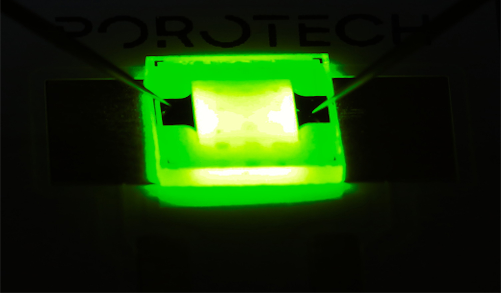
Porotech has created a new class of porous GaN semiconductor material that is redefining what is possible. It offers performance improvements that are suitable for mass production and can be customised for individual customers’ needs.
Despite only spinning out in January 2020, Porotech has been generating revenue for 10 months – and is working with some of the biggest global names in display technology. In November 2020, the company launched the world’s first commercial native red indium gallium nitride (InGaN) LED epiwafer for micro-LED applications.
Porotech will now work to expand its novel approach to integrate InGaN-based red, green and blue (RGB) micro-LEDs for full-colour microdisplays – and ultimately create ‘smart’ pixels that can be controlled independently for unrivalled responsiveness and accuracy for things like AR gestures.
Currently, technologies being tested for smart pixels are largely based on aluminum indium gallium phosphide (AlInGaP) material and quantum dot colour conversion (QDCC). But AllnGaP struggles at the small pixel sizes required by AR – and QDCC suffers from uniformity and stability issues. In addition, both approaches require a mixture of different materials.
Porotech’s novel approach enables all three primary colours to be made with the same GaN material and integrated on a single wafer, with no need for special structuring. The company also plans to develop its own supply chain ecosystem to help it develop and produce products more quickly.
“Porous GaN is basically GaN with tiny holes in it that are a few tens of nanometres across,” said Porotech CEO and co-founder Tongtong Zhu. “It’s an entirely new engineered GaN material platform to build semiconductor devices on. It offers performance improvements that are suitable for mass production, scalable in wafer size – and crucial for the next generation of microdisplay devices such as AR glasses.
“We are already seeing high levels of demand for our standard and customised porous GaN substrates and micro-LED epiwafers, which we can provide on sapphire and silicon platforms ranging from 100mm (4inch) to 300mm (12inch).
“Smart pixels will be our next development – monolithically generated and integrating native self-emissive RGB micro-LEDs on a single wafer to give smaller, lighter, thinner displays that use less energy and offer the greater accuracy required for things like AR gestures.”
Porotech’s latest funding round was led by Speedinvest, with participation from previous investors IQ Capital,Cambridge Enterprise, Martlet, and Cambridge Angels.
Rick Hao, principal at Speedinvest, said: “The revolutionary technology developed by Porotech is set to transform the electronics industry as demand grows for smaller, lighter, sharper displays that are more accurate and environmentally friendly than ever before.
“This new type of porous GaN semiconductor material fits within existing industry processes and is robust and flexible enough to be tailored to different applications. Porotech has demonstrated that it has both the product and the commercial capability to become a key player in next-generation display technology.”


