Loading...
News Article

ST Makes First 200mm SiC Wafers

News

Transition to 200m wafers marks milestone in capacity build-up to support automotive and industrial markets

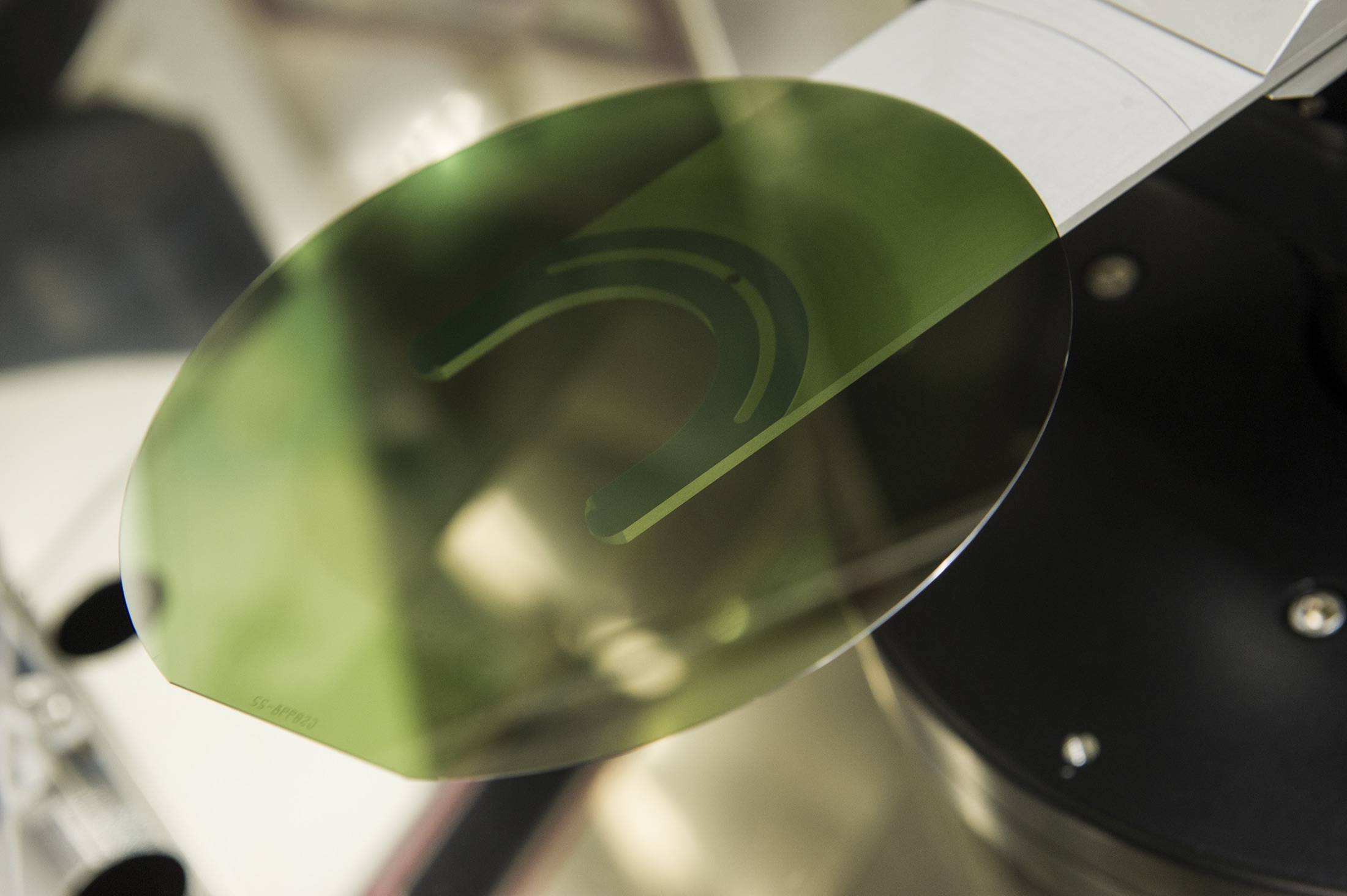
STMicroelectronics has announced it has manufactured the first 200mm (8-inch) SiC bulk wafers for prototyping next-generation power devices from its facility in Norrköping, Sweden.

The transition to 200mm SiC wafers marks an important milestone in the capacity build-up for ST’s customer programs in automotive and industrial sectors and will consolidate ST’s lead in the disruptive semiconductor technology that allows for smaller, lighter, and more efficient power electronics with a lower total cost of ownership.

Among the first in the world, ST’s initial 200mm SiC wafers are also very high quality, with minimal yield-impacting and crystal-dislocation defects. The low defectivity has been achieved by building on the excellent know-how and expertise in SiC ingot growth technology developed by STMicroelectronics Silicon Carbide A.B. (formerly Norstel A.B., which ST acquired in 2019). In addition to meeting the quality challenge, the transition to 200mm SiC substrates requires a step forward in manufacturing equipment and the overall support ecosystem performance. ST, in collaboration with technology partners covering the entire supply chain, is developing its own 200mm SiC manufacturing equipment and processes.

ST currently manufactures its high-volume STPOWER SiC products on two 150mm wafer lines in its fabs in Catania (Italy) and Ang Mo Kio (Singapore) and performs assembly and test at its back-end sites in Shenzhen (China) and Bouskoura (Morocco). This milestone comes as part of the Company’s planned move to more advanced, cost-efficient 200mm SiC volume production. This transition is within the Company’s ongoing plan to build a new SiC substrate plant and source over 40 percent of its SiC substrates internally by 2024.

“The transition to 200mm SiC wafers will bring substantial advantages to our automotive and industrial customers as they accelerate the transition towards electrification of their systems and products”, said Marco Monti, president Automotive and Discrete Group, STMicroelectronics. “It is important in driving economies of scale as product volumes ramp. Building robust know-how in our internal SiC ecosystem across the full manufacturing chain, from high-quality SiC substrates to large-scale front- and back-end production, boosts our flexibility and allows us to better control the improvement of yield and quality of the wafers.”

SPONSOR MESSAGE

Secure Your Hydrogen Supply

A study supply of high-purity hydrogen is critical to semiconductor fabrication. Supply chain interruptions are challenging manufacturers, leading to production slowdowns and stoppages. On-site hydrogen generation offers a scalable alternative for new and existing fabs, freeing the operator from dependence on delivered gas.

Plant managers understand the critical role that hydrogen plays in semiconductor fabrication. That important job includes crystal growth, carrier gas, wafer annealing, and in the emerging Extreme UV Lithography (EUV) that will enable new generations of devices. As the vast need for semiconductors grows across all sectors of world economies, so does the need for high-purity hydrogen.

Take control with Nel on-site hydrogen generation.

Read more
SiC MOSFETs: Understanding the benefits of plasma nitridation
Wolfspeed reports Q2 results
VueReal secures $40.5m to scale MicroSolid printing
Mitsubishi joins Horizon Europe's FLAGCHIP project
Vishay launches new high voltage SiC diodes
UK team leads diamond-FET breakthrough
GaN adoption at tipping point, says Infineon
BluGlass files tuneable GaN laser patents
QD company Quantum Science expands into new facility
Innoscience files lawsuit against Infineon
Riber revenues up 5% to €41.2m
Forvia Hella to use CoolSiC for next generation charging
Photon Design to exhibit QD simulation tool
Ortel transfers CW laser fabrication to Canada
Luminus adds red and blue multi-mode Lasers
PseudolithIC raises $6M for heterogeneous chiplet tech
Mesa sidewall design improves HV DUV LEDs
IQE revenue to exceed expectations
'Game-changing' VCSEL system targets clinical imaging
German start-up secures finance for SiC processing tech
Macom signs preliminaries for CHIPS Act funding
IQE and Quintessent partner on QD lasers for AI
EU funds perovskite tandems for fuel-free space propulsion
EU to invest €3m in GeSi quantum project
Transforming the current density of AlN Schottky barrier diodes
Turbocharging the GaN MOSFET with a HfO₂ gate
Wolfspeed launches Gen 4 SiC MOSFET technology
Report predicts high growth for UK's North East
Element Six unveils Cu-diamond composite
SemiQ launches hi-rel 1700V SiC MOSFETs
Lynred to exhibit Eyesential SWIR sensor for machine vision
Thorlabs buys VCSEL firm Praevium Research
×
Search the news archive

To close this popup you can press escape or click the close icon.
Logo
x
Logo
×
Register - Step 1

You may choose to subscribe to the Compound Semiconductor Magazine, the Compound Semiconductor Newsletter, or both. You may also request additional information if required, before submitting your application.


Please subscribe me to:


You chose the industry type of "Other"

Please enter the industry that you work in:
 
x
Adblocker Detected
Please consider unblocking adverts on this website