
Scientists build UV phototransistor with record responsivity
USTC team demonstrate high performance phototransistor based on the AlGaN/GaN HEMT configuration
The pursuit of the high-efficient ultraviolet photodetectors (UV PDs) has lasted for decades to meet the requirements in both civil and military applications such as fire alarm, space exploration, missile detection, secure communication, etc.
So far, various device structures of GaN-based UV PDs such as p-i-n, Schottky, and metal-semiconductor-metal (MSM) have been proposed and studied. In addition to those conventional configurations, an AlGaN(InAlN)/GaN heterojunction structure (the key building block for HEMTs) has gained attention.
Due to the inherent polarisation effects of III-nitride materials, there exist high-concentration and high-mobility two-dimensional electron gases (2DEGs) at the AlGaN/GaN hetero-interface. As a result, such UV PDs usually possess large photocurrent (Iphoto), high photoresponsivity (R), and transistor-like electrical and optical performance. However, the spontaneously formed 2DEG would lead to inferior noise performance, namely high dark current (Idark) and low detectivity (D*) during device operation.
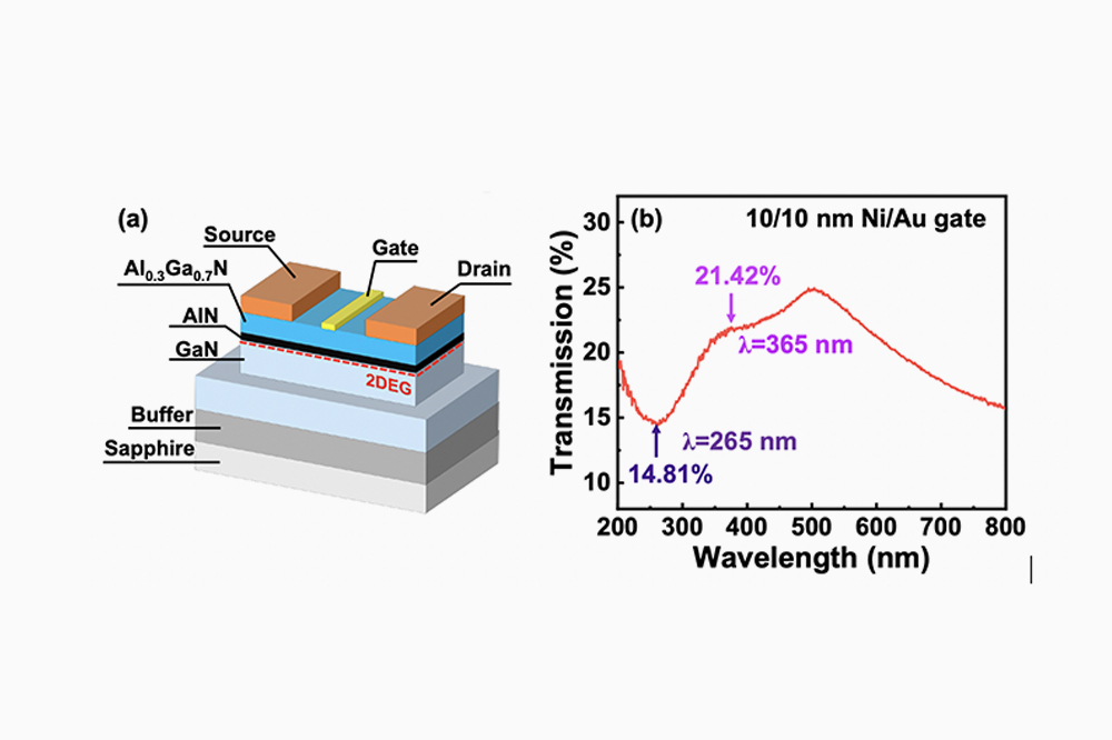
Recently, a team from University of Science and Technology of China (USTC) led by Haiding Sun and Shibing Long demonstrated a UVPT based on AlGaN/GaN HEMT configuration using a 10/10 nm Ni/Au semitransparent gate, as shown in figure 1 (at the top of the page).
When the device is biased at off state, a low dark current of 20 pA can be achieved. More importantly, a superior photodetection behavior can be obtained, featuring the peak R values of 3.6×10⁷ A/W under 265 nm UV illumination and 1.0×10⁶ A/W under 365 nm UV illumination, respectively. Those two values are the record high responsivity among the reported UV PDs at the same detection wavelength under off-state conditions. A further study in the VGS-dependent photoresponse of the UVPT reveals that a more negative VGS would significantly reduce the rise/decay time for 265 nm detection thanks to an increased electric field in the absorptive AlGaN barrier layer. In contrast, the VGS has little impact on the switching process for 365 nm detection since the GaN channel has a larger absorption depth and the device operates in the photoconductive mode.

Fig. 2. The transfer curves of the UVPT under (a) 265 nm and (b) 365 nm UV illumination with various incident power. (c) and (d) show the extracted and R and PDCR under different UV intensity.
The measured transfer characteristics of the UVPT under different light sources are plotted above in Fig. 2(a) and (b).
The UVPT should be operated at the off state. Therefore, they mainly focus on the electrical and optical properties under VGS (gate voltage) < Vth (threshold voltage) conditions. Under dark conditions, the device exhibits a low Idark on the order of ~pA at cut-off region and an ON/OFF ratio of 2.5×10⁸ at a drain voltage (VDS) of 8 V, which lays the basic foundation of a high-performance UVPT.
Additionally, the R and photo-to-dark-current ratio (PDCR) values of the UVPT under 265 nm and 365 nm illumination are extracted from the transfer curves at VGS = -8.2 V, where Idark reaches the lowest value of 20 pA. The maximum PDCR are obtained at the highest UV light intensity, i.e., 8.1×10⁷ for 265 nm at 3.75 mW/cm2 and 3.6×10⁷ for 365 nm at 7.00 mW/cm2. The peak R values are calculated as 3.6×10⁷ (265 nm, 12 μW/cm2) and 1.0×10⁶ (365 nm, 340 μW/cm2), respectively. It should be noted that R reaches the first peak value of 6.9×10⁵ under 365 nm UV light at 21.8 μW/cm2, as shown in Fig. 2(d).
This is possibly because the photo-induced carriers can only exist in the depleted channel at the AlGaN/GaN hetero-interface under weak light detection. When the UV intensity increases, the excess carriers are generated in the beneath GaN channel and a second R peak occurs under strong light illumination of 340 μW/cm2.
Furthermore, they observed a distinct difference between rise time (tr) and decay time (td) of the device under 265 nm and 365 nm light illumination which can be attributed to the unique device operating principle of the constructed AlGaN/GaN-based UVPT structure with different absorption mechanism in the device.
In the end, they mentioned that the device can be further improved by optimising the device structures, the growth techniques, ICP etching, post-etch treatment, and gate metal deposition schemes. Such superior photodetection behaviour of the AlGaN/GaN UVPT provides a feasible device architecture to promote the development of high-performance UV PDs based on wide bandgap semiconductors of the future.
Ref
Haochen Zhang, Haiding Sun et al., Appl. Phys. Lett. 118, 242105 (2021); https://doi.org/10.1063/5.0055468


