Small size improves DUV LED efficiency

USTC team shows how smaller chip size can deliver higher AlGaN-based DUV LED light output power density and peak external quantum efficiency
Deep ultraviolet (DUV) light source have numerous valuable applications, including germicidal irradiation, phototherapy, water/air/food sterilization, and optical communication. But while research on AlGaN-based DUV LEDs has made exciting progress, their industrial applications are still in their infancy.
This is because of their limited wall plug efficiency (WPE) which is cause by low external quantum efficiency (EQE), the deprived light extraction efficiency (LEE), and the severe current crowding effect in the large chips.
Significantly, these LED characteristics strongly depend on the chip size, which has been widely investigated in visible LEDs. However, such studies have not been carried out in the DUV micro-LED devices.
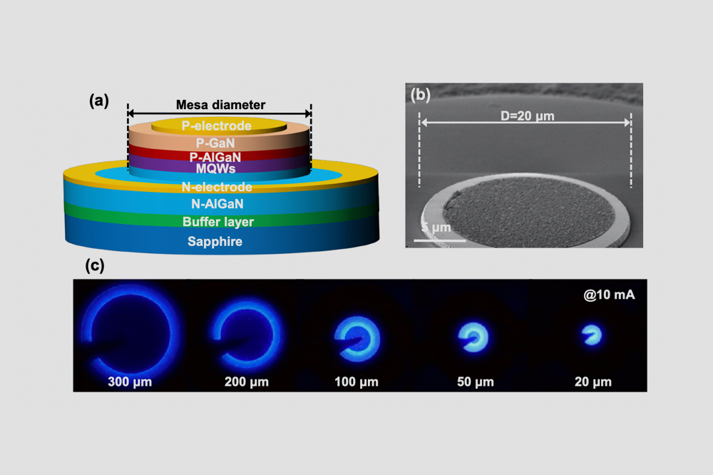
Recently, a team from the University of Science and Technology of China (USTC) led by Haiding Sun investigated the size dependence of the optical and electrical properties of 275 nm DUV micro-LEDs with an emphasis on the fabricated devices having a diameter (D) of 300, 200, 100, 50, and 20 μm, respectively. The schematic of the fabricated devices is shown in Figs. 1(a) at the top of the article.
The scanning electron microscopy (SEM) image of the LED with a diameter of 20 µm and the optical micrographs (top view) of the five-group LED emission patterns are shown in Figs. 1(b) and 1(c). It has been revealed that the smaller DUV micro-LEDs offer higher power densities, and higher EQE can be achieved at high injection current densities as a result of the improvement of current spreading and light extraction efficiency (LEE).
Figure 2: (a) The J-V plots and (b) J-V plots in log scale of the LED chips with a diameter of 20, 50, 100, 200, 300 μm, respectively. (c) Power density, and (d) external quantum efficiency (EQE) against current density for the DUV LEDs with different sizes.
Interestingly, the smallest LED with a diameter of 20 µm can sustain a very high forward current density, reaching over 4500 A/cm2.
A logarithmic plot of the forward J-V curves is presented in Fig. 2(b), from which we can observe that the leakage current of the devices also shows a size-dependent behavior. As a result of the higher surface-area-to-volume ratios, the leakage current of the LEDs with a smaller mesa size tends to be larger as the sidewall defects near the edge of the mesa could possibly act as current leakage paths.
Moreover, they normalized the light output power with the LED p-electrode size at different injection currents and plotted the power densities as a function of the current densities in Fig. 2(c). Intriguingly, the LEDs with smaller mesa areas can deliver higher power densities under the same current densities. Such power density improvement in the smaller chip is mainly due to a better uniformity of the current spreading. It is also noteworthy that the smallest devices (D=20 µm) provide the highest maximum power density of up to 86 W/cm2, which is over 20 times higher than the value in the largest device (D=300 µm) with a maximum power density of 4.14 W/cm2. Subsequently, the EQE values of the LEDs were extracted from light output power measurements.
As plotted in Fig. 2(d), among those large LEDs (D≥100 μm), the LEDs with smaller diameters show the lower EQE values at low current densities. As a matter of fact, the ratio of sidewall perimeter to mesa area for 100 μm LED is three times that of 300 μm LED and thus, more defect-related non-radiative recombination on the edge of mesa sidewalls could be expected, which possibly contributes to the suppression of the radiative recombination as it is highly sensitive to the sidewall defects.
Consequently, the EQE values in those LEDs (D≥100 μm) at low current densities are lower in those LEDs with a smaller diameter but higher at larger current densities because of a better uniformity of current spreading. When it comes to small LEDs (D<100 μm), they found that the small LEDs overall have higher EQEs than that of those larger LEDs (D≥100 μm), attributing to a better uniformity of current spreading as well as a possible higher LEE.
The enhanced LEE for the smaller LED chips is attributed to the strong wave-guiding effect in the AlGaN multilayers and the low power loss in the shorter optical path of the emitted photons inside the LED chip. Moreover, when the device diameter is reduced, more light can reflect off the mesa sidewalls, thus further enhancing the light extraction. In addition, they observe a strong peak wavelength redshift and the increment of full width at half maximum (FWHM) values in those micro-LEDs due to self-heating under high current injection.
In the end, they mentioned that in the deep ultraviolet band, the entire DUV LED community still faces big challenges to find an effective way to further enhance the EQE performance. Their micro-LED design and fabrication could offer an alternative approach to boost the EQE of DUV LEDs by fabricating small LED arrays in series or in parallel to replace the conventional big single LED chip.
This work offers a comprehensive understanding of the electrical and optical performance of DUV micro-LEDs, in particular, these experimental observations provide insights into the design and fabrication of high-efficiency micro-LEDs emitting in the DUV regime with different device geometries for various future applications.
Ref
Huabin Yu, Haiding Sun et al., Opt. Lett. 46(13), 3271-3274 (2021)


