
Reducing the operating voltage of tunnel-junction deep UV LEDs
Driving down carbon contaminations and cranking up silicon trims the operating voltage of deep-UV LEDs with a tunnel junction
A Japanese collaboration is claiming to have broken new ground for reducing the operating voltage of tunnel-junction deep-UV LEDs. Success has come from suppressing the incorporation of carbon contaminants in an n-type AlGaN layer that is then doped with a high concentration of silicon.
The lower operating voltage promises to increase the optical efficiency of high-power tunnel-junction LEDs, which will become the dominant form of this device, according to Kengo Nagata, spokesman for the team. Nagata, who is affiliated to Nagoya University, Toyoda Gosei and TS Opto, told Compound Semiconductor that it is extremely difficult to realise an ohmic p-type AlGaN contact. “We believe that the tunnel-junction LED is one of the device structures that solves this problem.”
Note that switching to GaN for the p-contact is not a viable option. GaN would absorb light emitted by the quantum well, and drive down the light extraction efficiency for the deep-UV LED.
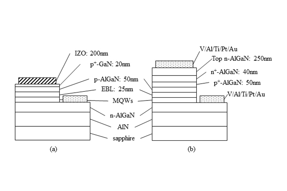
To uncover good growth conditions for lowering the operating voltage of deep-UV LEDs with a tunnel-junction, the team from Nagoya University, Toyoda Gosei, TS Opto and Meijo University produced a portfolio of devices. As well as making a pair of devices with a p-n junction that has different aluminium concentrations in the p-AlGaN layer, they fabricated five devices with tunnel junctions containing differing levels of carbon and silicon concentrations in the n+ AlGaN and top n-AlGaN layers (see Figure for details of both structures).
All these forms of deep-UV LED were produced on sapphire substrates with a 3 µm-thick AlGaN template that had screw and edge dislocation densities of
9 x 107 cm-2 and 1 x 109 cm-2, respectively. On this the team added an n-type Al0.38Ga0.62N underlayer, with screw and edge dislocation densities of 1 x 108 cm-2 and 9 x 108 cm-2, followed by an active region with 2 nm-thick Al0.45Ga0.55N quantum wells and an electron-blocking layer.
After adding either a p-GaN/AlGaN structure or a tunnel-junction, 1 mm2 LEDs were formed by using dry etching to define a mesa, prior to adding contacts. A stack of metals provided both of the n-AlGaN contacts for the tunnel-junction LED, as well as the n-AlGaN for the p-n LED; while an indium zinc oxide layer provided the p-GaN contact for the p-n LED.
Current-voltage plots for the p-n junction LED produced typical results for this class of device, with a forward voltage of 6.6 V at 63 mA cm-2.
Comparing current-voltage characteristics for a variety of deep-UV emitters with tunnel-junctions revealed that a reduction in the level of carbon contaminants, realised by lowering the growth pressure from 100 mbar to 50 mbar, reduced the operating voltage by more than 6 V. Combining this with a high silicon-doping concentration in the n+ AlGaN layer led to an additional and significant reduction in operating voltage to 10.3 V at 63 mA cm-2. Getting the level of carbon contaminants down proved crucial, because it prevented the AlGaN layer from being semi-insulating – that is a show-stopper for forming a tunnel junction.
Optical measurements showed that the conventional UV LED produced an output of 35.7 mW at 285 nm, for a drive current density of 63 mA cm-2, realised at 7.2 V forward voltage. The tunnel-junction device providing a comparison realised an identical drive current at 10.8 V, and delivered an output of 27.6 mW, for a peak emission wavelength of 280 nm. The team attributed this inferior performance to high absorbance by the n-type electrodes, which were sintered at a high temperature.
Nagata says that one of the goals for the team is to extend the optimisation of the tunnel junction, with efforts directed at improving the growth conditions for other layers. “In addition, we will take on the challenge of improving device characteristics, using reflective electrodes.”
Pictured at the top of the page: The epistructure used for conventional deep-UV LEDs and those with a tunnel junction.
Reference
K. Nagata et al. Appl. Phys. Express 14 084001 (2021)


