
Improving ohmic contacts for Ga2O3
Low-temperature MOCVD re-growth creates Ga2O3 MESFETs with record-breaking currents and on-off ratios
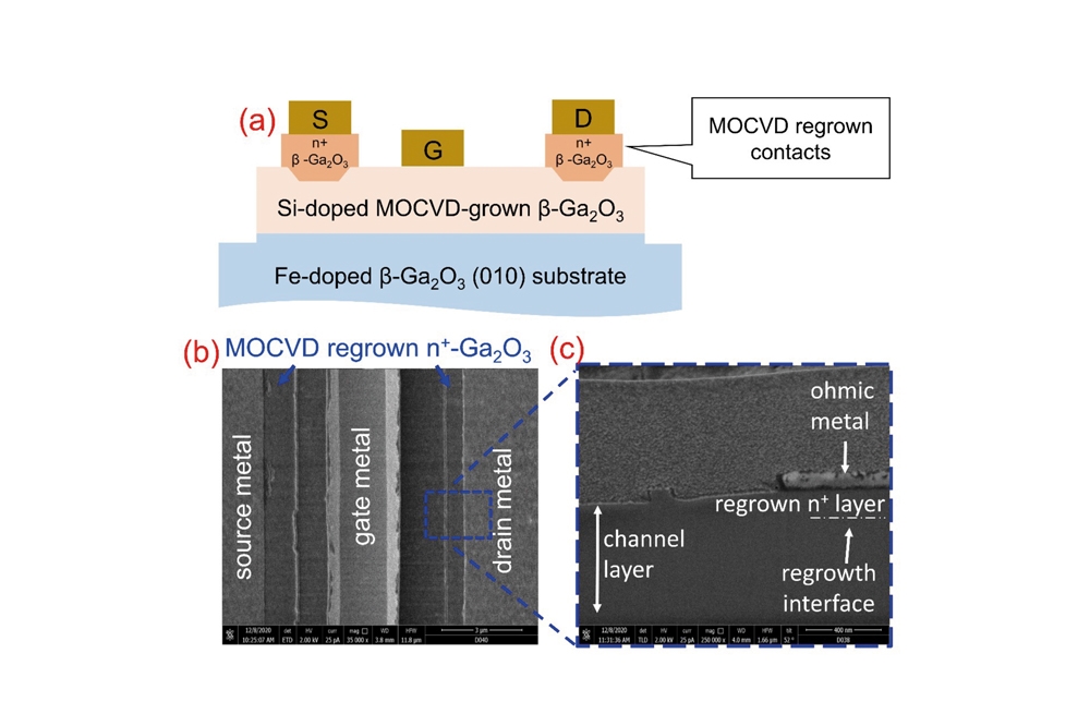
A collaboration between engineers at the University of Utah and The Pennsylvania State University claims to have produced the first fully MOCVD-grown B-Ga2O3 MESFETs with ohmic contacts.
Spokesman for the team, Sriram Krishnamoorthy from the University of Utah, told Compound Semiconductor that a major bottleneck for re-growing ohmic contact is the need for high temperatures, to ensure high-quality material. These high temperatures threaten to degrade the channel. “We came up with a solution and demonstrated high-quality B-Ga2O3 growth using MOCVD at a temperature of 600 °C, which is more than 200 °C lower than the conventional growth temperatures for MOCVD Ga2O3 growth.”
As well as reducing the thermal budget, the lower growth temperature opens up avenues for hetero and hybrid integration with other semiconductor materials that require lower processing temperatures.
Growth of B-Ga2O3 at lower temperatures also enabled controllable doping over four orders of magnitude, and doping profiles ten times sharper than before. “This could help in the development of high-efficiency Ga2O3-based lateral RF devices through delta doping and modulation doping schemes,” argued Krishnamoorthy.
The team produced their devices using a Agnitron Agilis MOCVD reactor, which is specifically designed for high-quality growth of B-Ga2O3 material on wafers
with sizes up to 2 inch. Efforts began by taking iron-doped semi-insulating B-Ga2O3 substrates produced by NCT, Japan, cleaning their surface by dipping them in a dilute HF solution for 30 minutes, and then loading this material into an MOCVD chamber and depositing a 500 nm-thick B-Ga2O3 channel at 810 °C. Device mesas were defined by a hard mask and dry etching, before a selective area MOCVD regrowth process provided low ohmic resistance source and drain contacts.
Formation of these contacts began by adding a 500 nm-thick sacrificial layer of SiO2 by plasma-enhanced CVD. The source and drain regions were defined using a nickel layer patterned by photolithography and lift-off. Reactive ion etching selectively removed the SiO2, plus 10-20 nm of Ga2O3.
Dipping the sample in aqua regia solution removed the nickel mask, before the growth of silicon-doped Ga2O3at 600 °C. The next steps involved removing the polycrystalline Ga2O3 outside the contact region by dissolving the sacrificial SiO2 in HF solution, and using photolithography and patterning to add metallic contacts to the regrown contacts. Adding a metal stack for the Schottky gate completed fabrication.
According to the team, electrical measurements on their MESFETs revealed a record sheet resistance of 73 Ω/square for silicon-doped -Ga2O3 regrown layers, and a record-low specific-contact-resistance of 8.3 x 10⁻⁷ W cm2 for the metal/ B-Ga2O3 contacts. The on-current hit 130 mA m-1. “This is the highest [value] for a depletion mode B-Ga2O3 MESFET with an on-off ratio of over 1010, simultaneously in a large gate length device,” said Krishnamoorthy.
He explained that B-Ga2O3 lateral FETs suffer from an off-state leakage through the epilayer/substrate, due to residual silicon impurities. It is speculated that this problem originates from the wafer polishing process. “We have demonstrated an efficient way to suppress off-state leakage using pre-growth wafer cleaning, but have preserved the high-mobility of carriers in the MOCVD-grown channels.”
One goal is to now develop B-Ga2O3 scaled devices using MOCVD-grown channels that would leverage the high mobility of carriers for high-frequency applications. “We would also like to work on electric-field management techniques to further enhance the breakdown performance of MOCVD-grown B-Ga2O3 for high-power applications,” added Krishnamoorthy.
The picture above shows: (a) Fully MOCVD grown MESFETs with regrown ohmic contacts. (b) Top view, scanning electron microscopy image of the MESFET, showing the re-grown access regions. (c) Cross-sectional scanning electron microscopy image of the contact region.
REF
A. Bhattacharyya et al. Appl. Phys. Express 14 076502 (2021)


