
Hong Kong team develops monolithic InP/SOI platform
Researchers selectively grow InP sub-micron wires and membranes on SOI wafers using novel method
In a new paper published in Light Science & Application, a research team led by Kei May Lau and postdoc researcher Yu Han from the Photonics Technology Center of the Hong Kong University of Science and Technology, have developed a monolithic InP/SOI platform to simultaneously meet the three critical requirements.
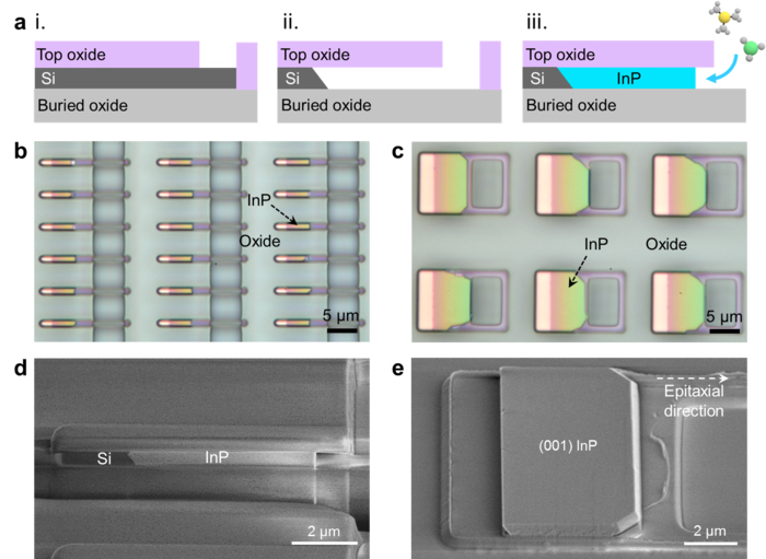
In their approach, both InP sub-micron wires and large dimension membranes are selectively grown on (001) SOI wafers using a novel growth method: lateral aspect ratio trapping. First, the defect necking effect of this approach results in dislocation-free InP on SOI. Second, large-area InP membrane is obtained via creating ultra-deep lateral oxide trenches and changing the growth direction from the prevailing vertical to lateral. Third, the epitaxial InP manifests an in-plane configuration and is positioned intimately with the Si device layer, which promotes efficient light interfacing.
In addition, the InP sub-micron wire array and large dimension InP membranes feature a unique InP-on-insulator (InPoI) characteristic and, similar to silicon-on-insulator, represent an ideal platform for implementing photonic functionalities. The authors exemplified the potential and versatility of this unique InP/SOI platform through the demonstration of optically-pumped lasers with different cavity designs, including subwavelength Fabry-Perot cavity, square cavities, and micro-disks.
Depending on the targeted device functions, the InP membranes can serve as templates for the regrowth of a variety of III-V structures for light emission, modulation and detection. For example, buried hetero-structure including InGaAs quantum wells and InAs quantum dots could be formed through selective vertical regrowth.
The InP sub-micron wires, formed through the replacement of Si sub-micron fins, are said to be ideal building blocks for subwavelength PICs and could also potentially enable the close integration with Si-based nano-electronics.
In addition, the InPoI resembles InP directly bonded onto oxide layers, and accordingly the InP/SOI platform could benefit from the well-established processing technologies developed in the III-V heterogeneous integration approach.
The picture above shows: a) Cross-section schematic of selective lateral heteroepitaxy of InP, b) InP sub-micron wire array, c) Large dimension InP membrane array, d) In-plane InP grown from {111} Si facet, and e) InP membrane on SOI.
'A monolithic InP/SOI platform for integrated photonics' by Zhao Yan et al; Light: Science & Applications volume 10, Article number: 200 (2021)


